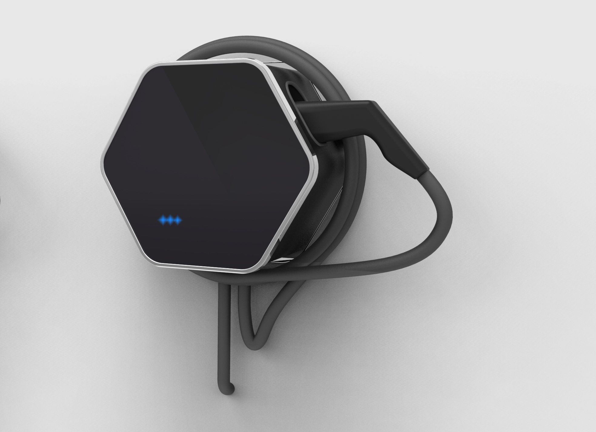
We thought a lot about the user interface for our charging station. After ditching the infinite mirror idea, we wanted something simple and elegant, inspired from the Tesla wall charger, so we started experimenting with RGB LEDs strips. The first version of the cover for the plastic case was a laser-cut polycarbonate sheet, with a LED-strip taped to the back:
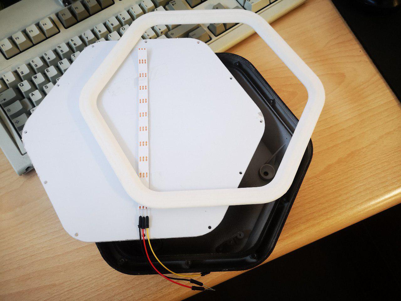
This plastic sheet can be easily UV printed for customization, but it’s a bit expensive to manufacture in big quantities. I was also a bit skeptic of this solution, as that kind of plastic is not very strong, especially on the thin borders around the screws. And we know that electricians installing this would drive the screws to death, cracking the cover and resulting in expensive returns.
Turns out, as the law of the instrument states, if you only have a hammer all problems look like nails, and my hammer is electronics. And, uhmmm, what item do I daily use that is a strong, thin, semi-transparent sheet, that is also cheap, widely available, easily customizable for design and color, embeds a metal shield to better comply with emission requirements (or can be etched to become an antenna!) and can host electronics easily? You guessed it: a PCB!
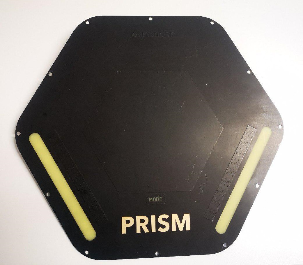
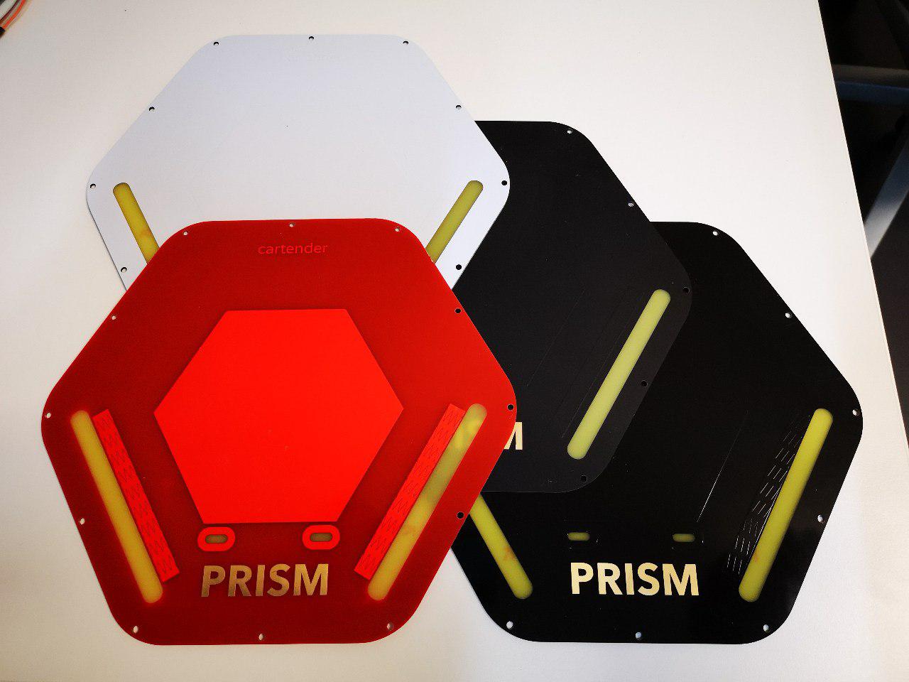
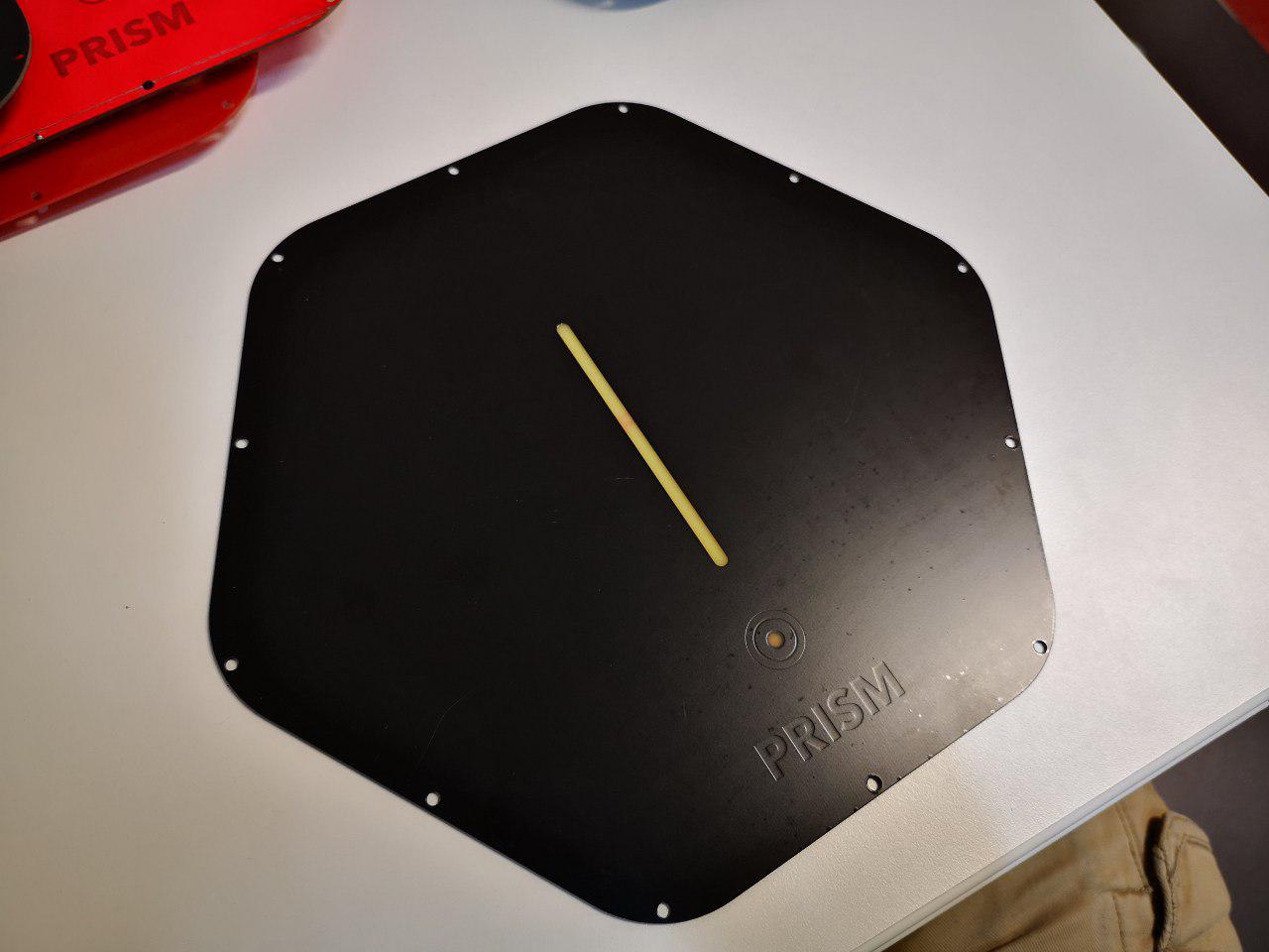
This is the first prototype of that idea. The “PRISM” logo is still gold-plated copper, but with the solder mask removed. I really like the matte black/gold combination. The two slots for LED strips and the MODE button are just the bare fiberglass base, with no copper and solder mask on both sides. There’s copper around the Mode button and near the LED slots for a touch button and touch sliders, controlled by a Silicon Labs CPT112S chip.
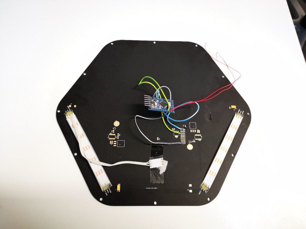
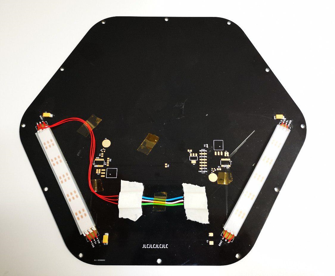
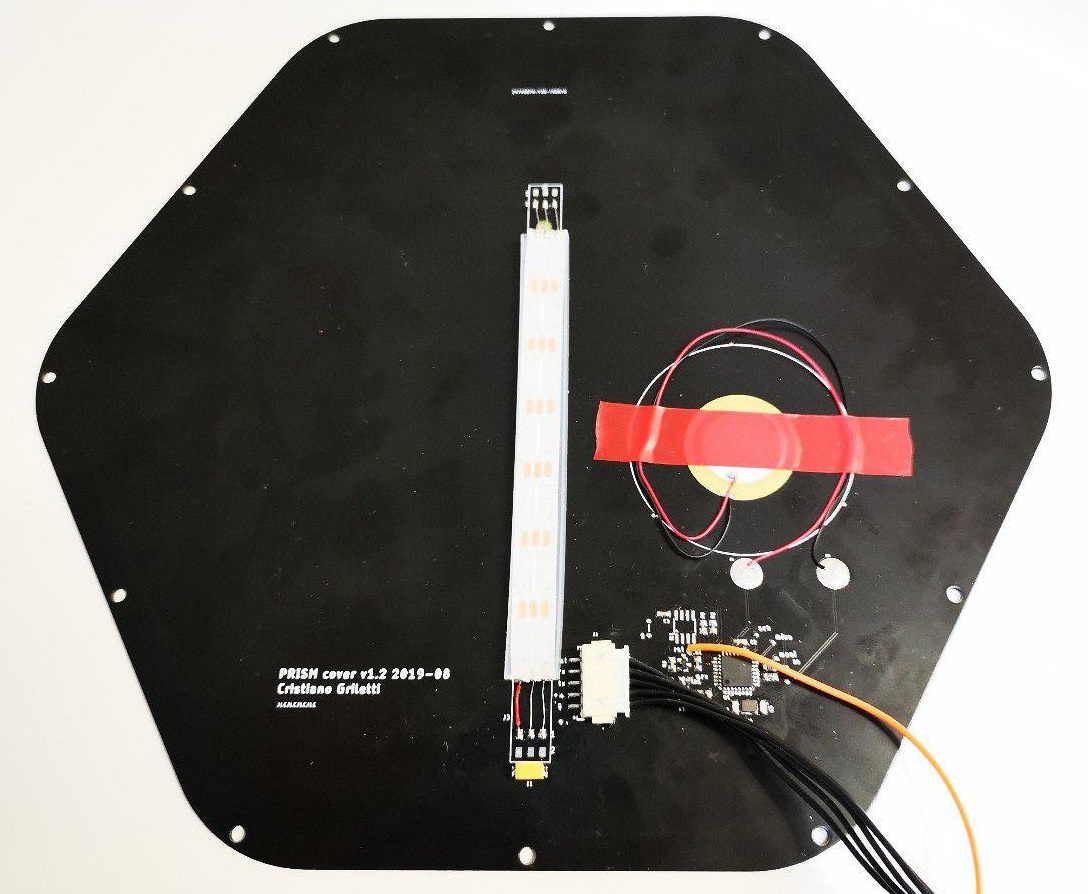
On the back, we have space for a connector to drive the LEDs and the I2C touch sensors. Here I connected it to an Arduino to test the look and feel of this solution:
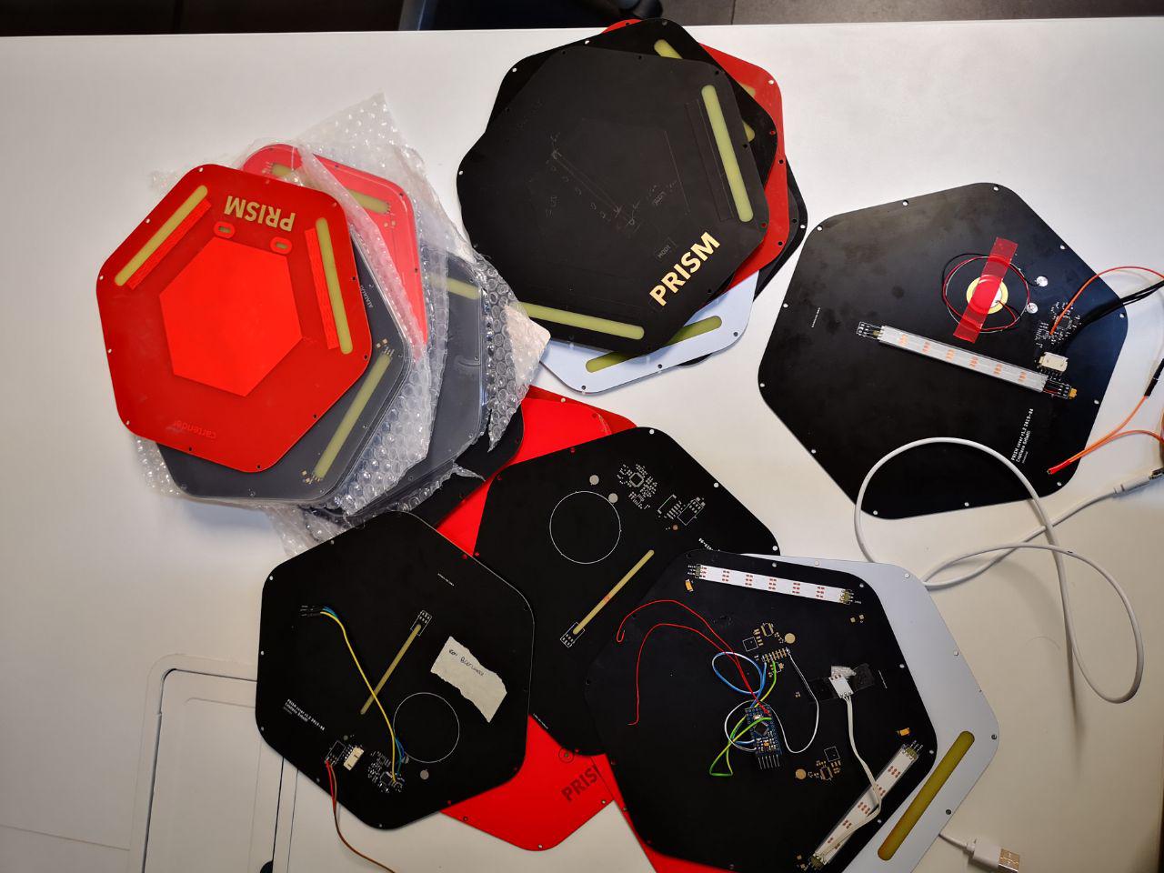
I soon prepared another revision, adding another Mode button (but without the text) and testing a bunch of different colors. The red soldermask is looking really nice as it brightly shows the copper layer underneath!
Here’s the back side and a video demo:
With the basic principles defined, we decided to improve the design by ditching the touch sliders and simplifying the lines:
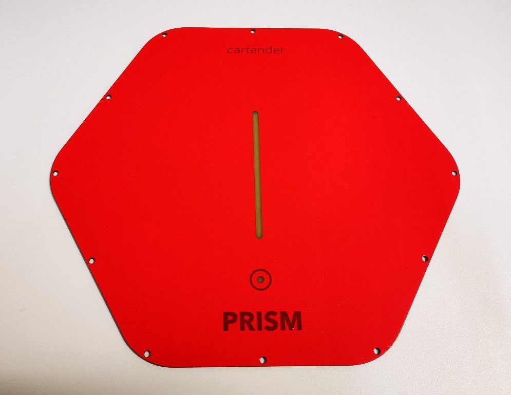

With no need for complex Touch ICs, I simply switched to a cheap CAP1203. Having three separate inputs, I connected the central copper areas of the “P” and “R” letters in PRISM to the spare touch input pins; the idea was to use a combination of the main and the “R” buttons to reset the device and/or to trigger easter eggs.
Instead of two separate LED strips and two additional LEDs for the buttons, I used a single central strip, hiding the second LED from the bottom to avoid having to solder many separate pieces of strip like in the early prototypes. It’s a waste of a LED, but it dramatically improves assembly time and it’s well worth the few cents, at least for the first small production batch.
I also added an ATmega328P to control everything: while the initial idea was to have just the LED strip controlled by the main board, this allows for greater flexibility and a nice gateway to start getting confident in reprogramming Prism. Even if you’re a newbie and you’re scared of playing with dangerous high voltage, you can still easily and safely customize the front panel with the familiar Arduino IDE. And we have a lot of ideas for that! Like making a Supercar themed version with a horizontal LED strip, a Larson scanner and cool black/gold graphics, or a HAL9000 version with a NeoPixel ring and a speaker to creep you out every time you plug your EV :)
But here comes a big fail: the CAP1203 touch IC doesn’t work with a wet sensor, and Prism will be installed and operated outside under any weather condition! We’re still discussing about the usefulness of that button (Prism is plug and play) anyway.
However this was a blessing in disguise, as being a big feature creep victim gave me the idea of adding a piezo disc to the cover. This way, we can have both a speaker and a knock sensor!
Looking around for inspiration, I only found projects using the piezo as either a sensor or a speaker; I couldn’t find any doing both. But that’s not hard: I connected the piezo to pins 9 and 10 of the Arduino, with a 100ohm resistor in series to limit driving current and a 1M resistor across it to limit output voltage.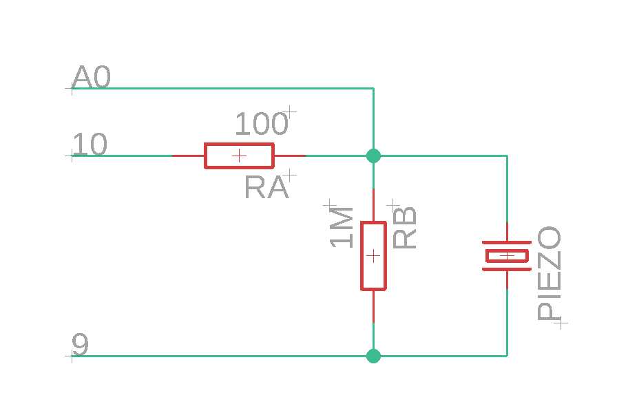 I’m connecting the piezo to two pins to drive it with twice the voltage using the toneAC library. I could barely hear the difference as human ears are logarithmic, but measuring with an app clearly showed double the sound pressure compared with the piezo driven only by a single pin. To sense a knock, we have to pull pin 9 to ground, make pin 10 an input and read the analog value from A0. We just have to wait a few milliseconds for the piezo to settle after playing a note before listening to knocks to avoid a loop.
I was a bit worried about the voltage spikes from the piezo, but the internal ATmega protection diodes seem to be enough to dissipate the tiny currents generated. I was also worried that wall vibrations from nearby passing trucks could generate false knocks, but it turns out that our rubber seals work very well to isolate vibrations too; I added a sensitivity setting to help in noisy environments if needed.
Here’s how it works, with some Super Mario nerdiness [source code here]:
And I can also program it to respond to different knock combinations, like this. It shouldn’t be hard to write some code to record custom knock sequences!
But I also didn’t want to give up the touch button yet, so I ditched the fancy ICs and implemented the TouchLib OpAmp circuit with a shielded sensor, that will hopefully work better with water.
And here it is, the latest version, in all its glory:
And it only took a few tries! :P
Why?
While engineering this cover, I had a big doubt stressing me the whole time. Why does no commercial product have PCBs exposed to the users? Sure, there are a few exceptions, but it’s mostly niche stuff. Am I missing something obvious?
There’s very few literature online about this, and basically people suggest you contact some external certification laboratory. Which I did, and while they said there shouldn’t be any problem, they also said I’d have to bring the product in and pay for testing to get a definitive answer, risking a negative verdict and wasting all the effort made in designing the cover (we’re still a team of two working on this, it would kill us). I wanted to be a bit more safe before committing to this, so I contacted the biggest expert on product development I knew: the great Bunnie. Here are the concerns he raised:
His answer was definitely encouraging, except for the ESD issue. After a lot of testing I was pretty confident that the PCB alone would have worked, but I’m a coward (and I invested too much on this) so I chickened out and designed an adhesive plastic sheet to cover the front of the PCB. Oh, and there’s another reason for this choice: it doesn’t happen very often, but sometimes the slots in the layers get aligned with visible markings on the bare FR4 board, clearly visible from the back but barely visible from the front. I can probably arrange something with the manufacturer if I have to order huge quantities, but for now I don’t want to risk scrapping a lot of boards so the front adhesive is still the best option, despite costing like the PCB, doubling the cost of this part.
I have two options here, a great-looking 0.5mm thick sheet that would force me to reduce the PCB thickness to 1.2mm to still fit in under the frame, or a 0.2mm thick one that would barely fit. I should get some samples soon, we will see what looks best!
In the meantime, get the sources and everything you need to design your own custom front panel here! In the repo you can also a version with copy-pasted parts from the Adafruit NFC reader to play around with the idea of embedding a card reader on the cover, but I haven’t completed that design yet. You can also play around with the firmware here (hey! help us implement custom knock sequences! :) )