 This article is part of a larger project to build a multi-purpose board that can replace a Nokia 3310′s mainboard.
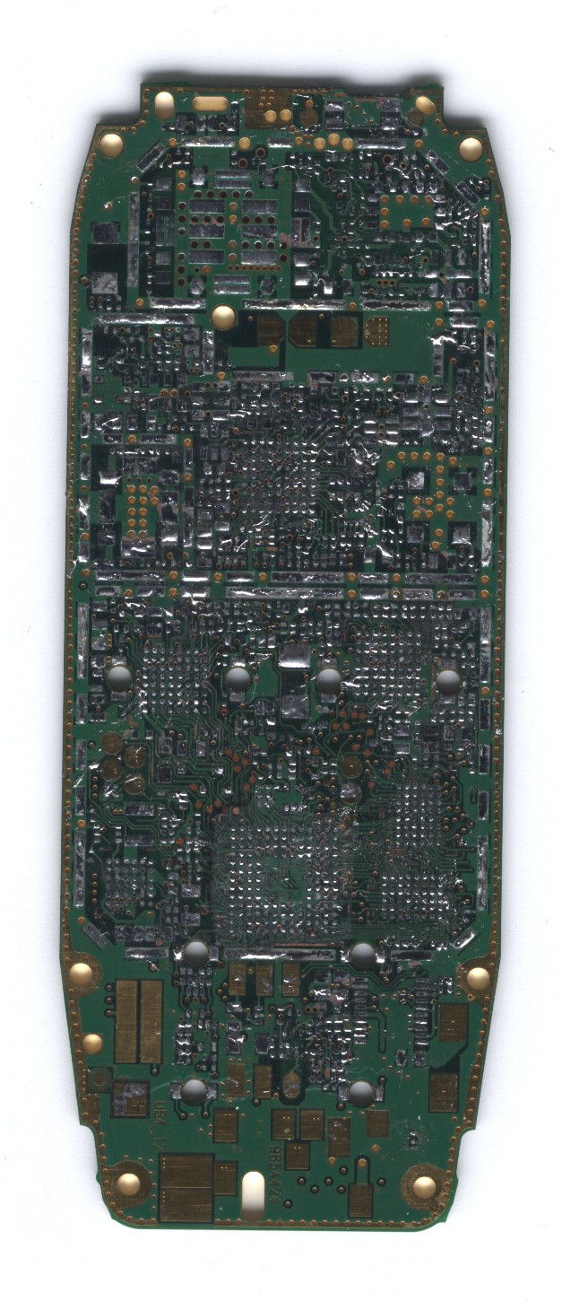
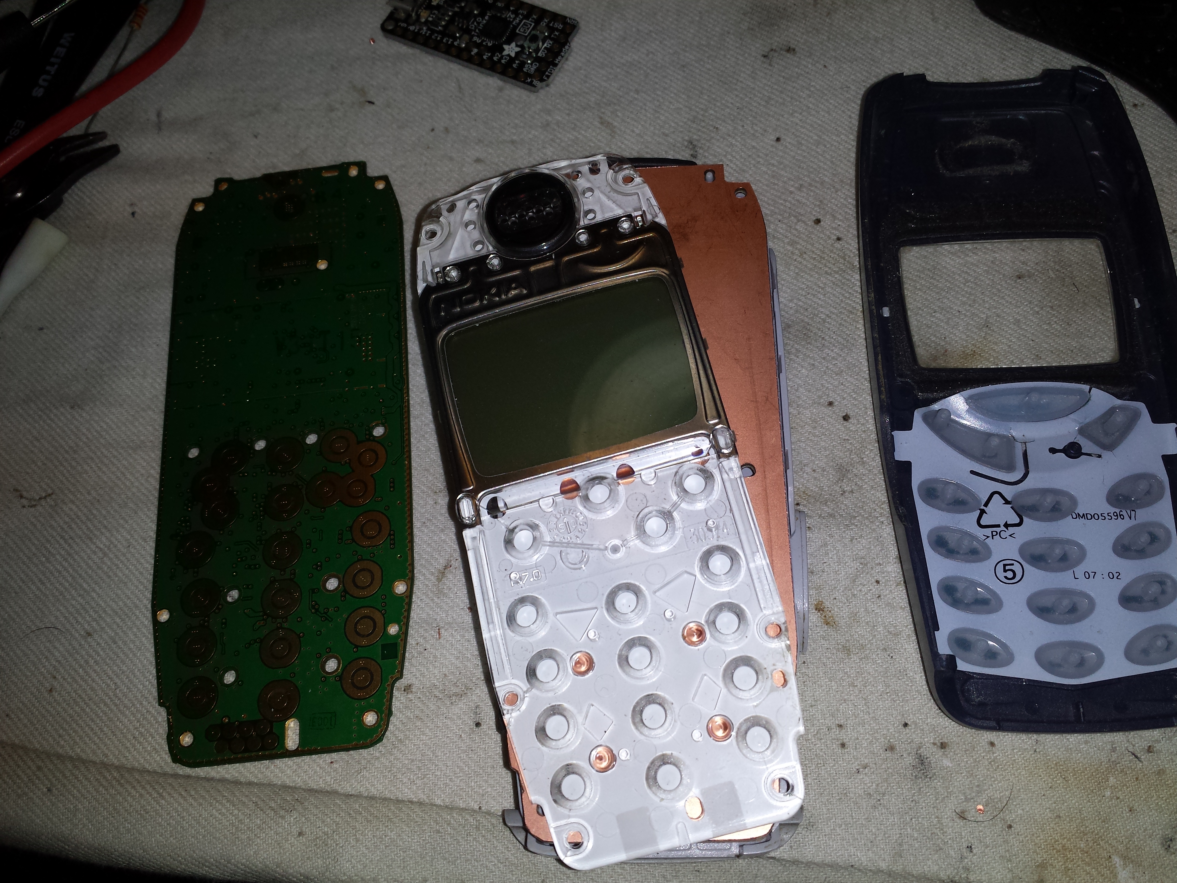
Designing a replacement PCB for the 3310 mainboard requires quite a bit of effort. The first thing I did was to remove all the components from a broken phone, to get a nice scan of the board:
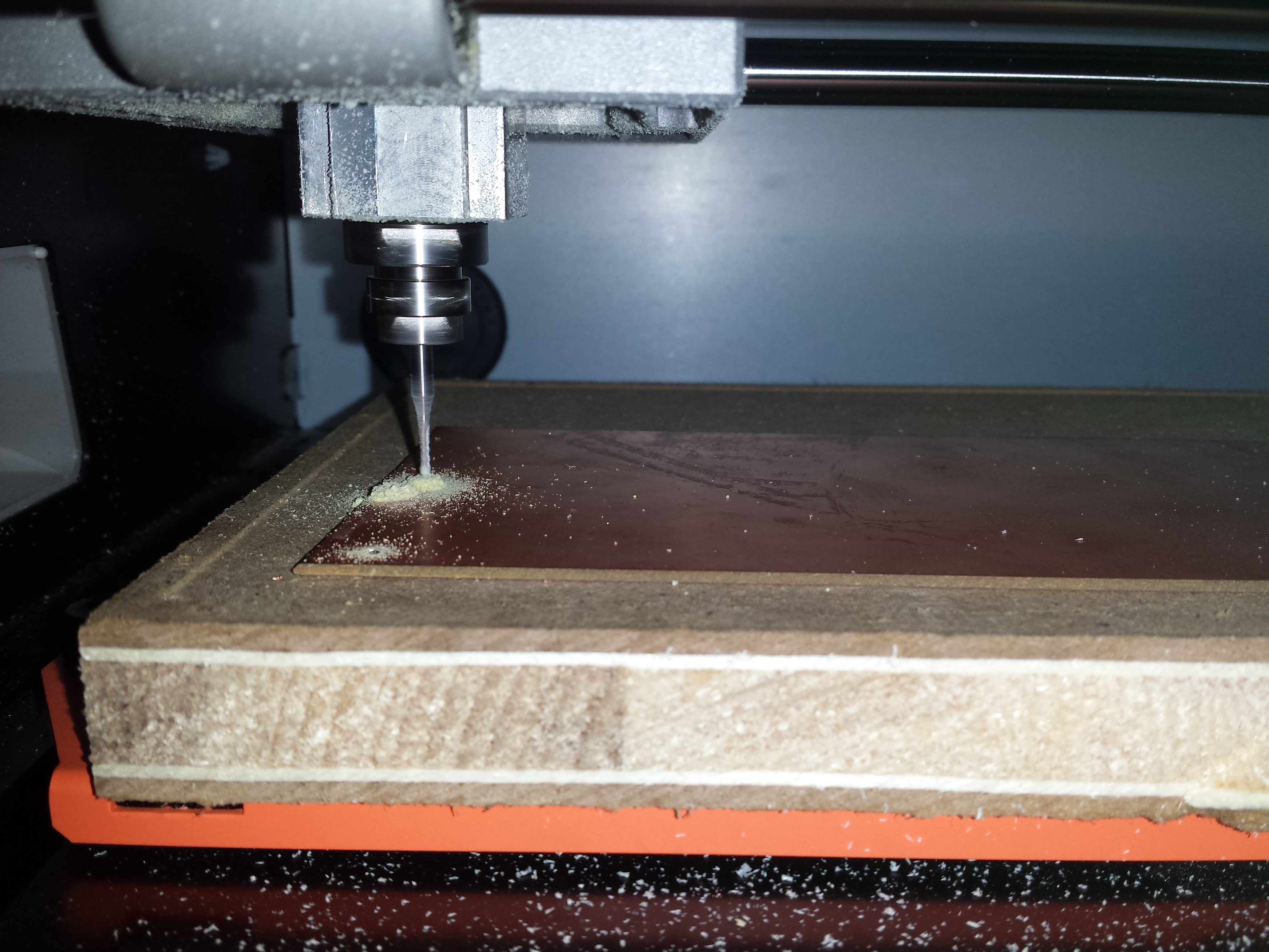
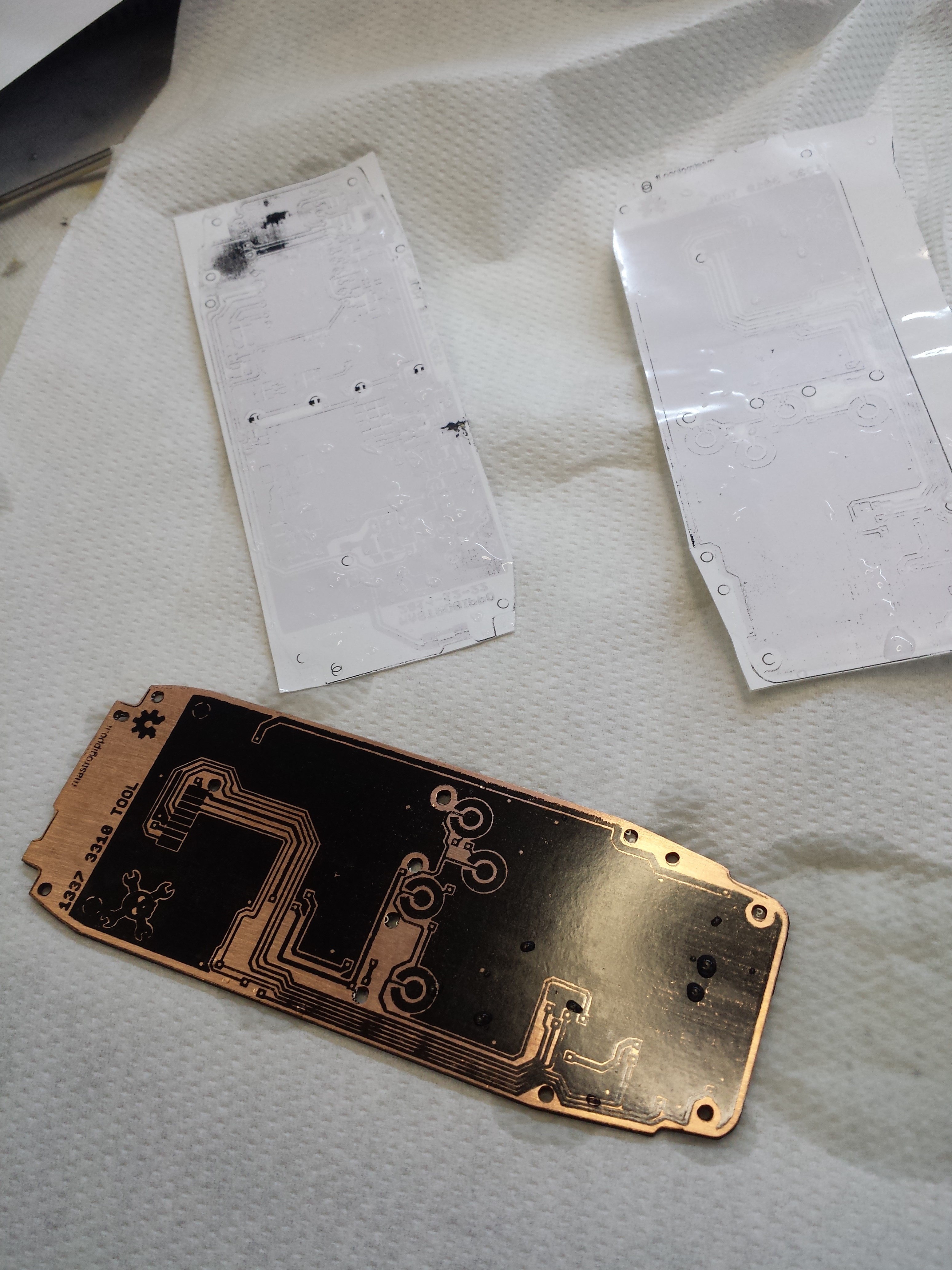
Now I know where all the holes and pads are, and I can draw the outline of the PCB. After a lot of failed attempts and frustration with various open source softwares, I ended up using Adobe Illustrator to create an exportable vector image of the outline and holes to feed to my Roland SRM-20 mill. Here she is cutting the PCB to size:
 and here’s the result, after a lot of tests on foam to fix minor issues:
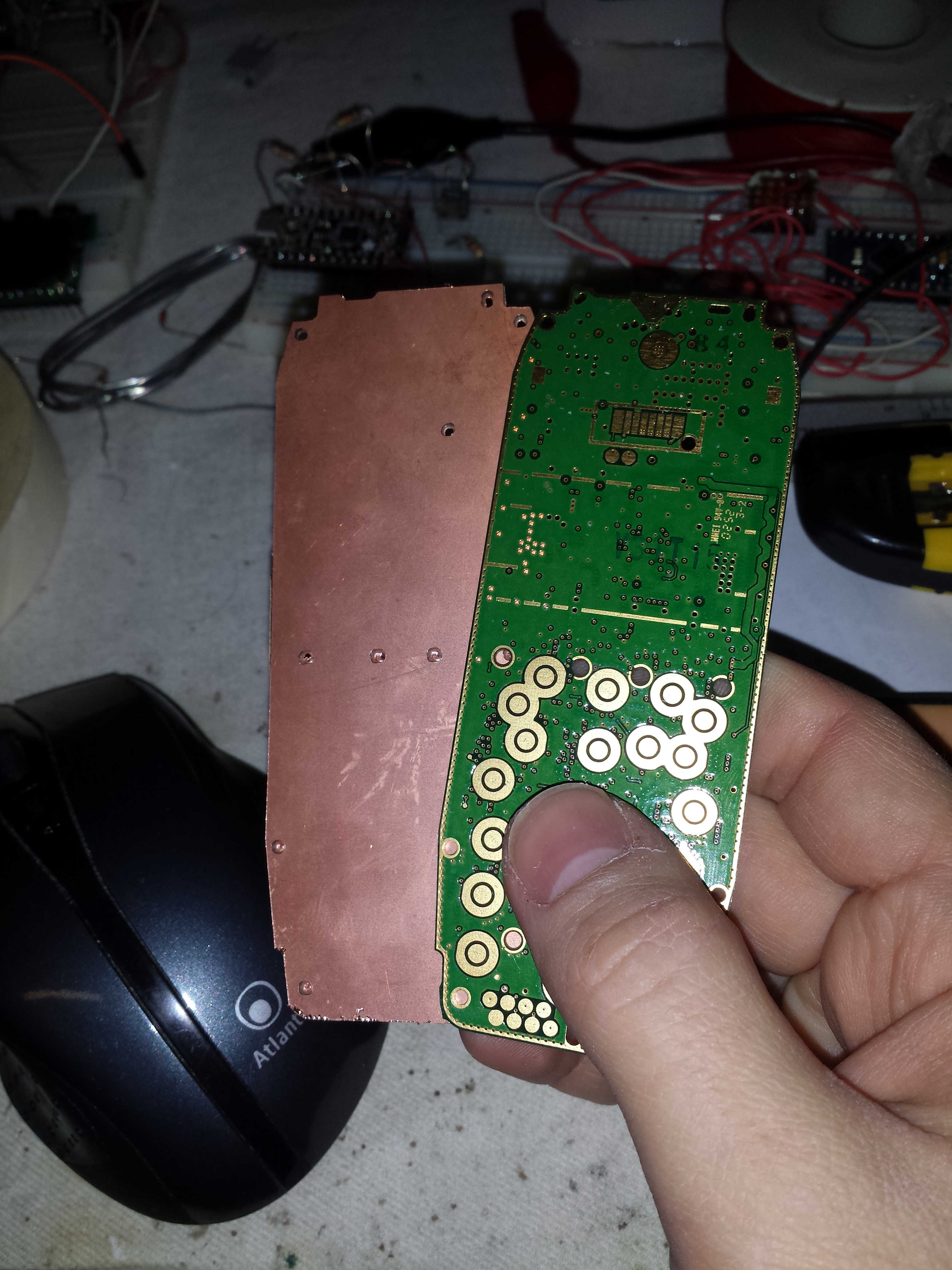
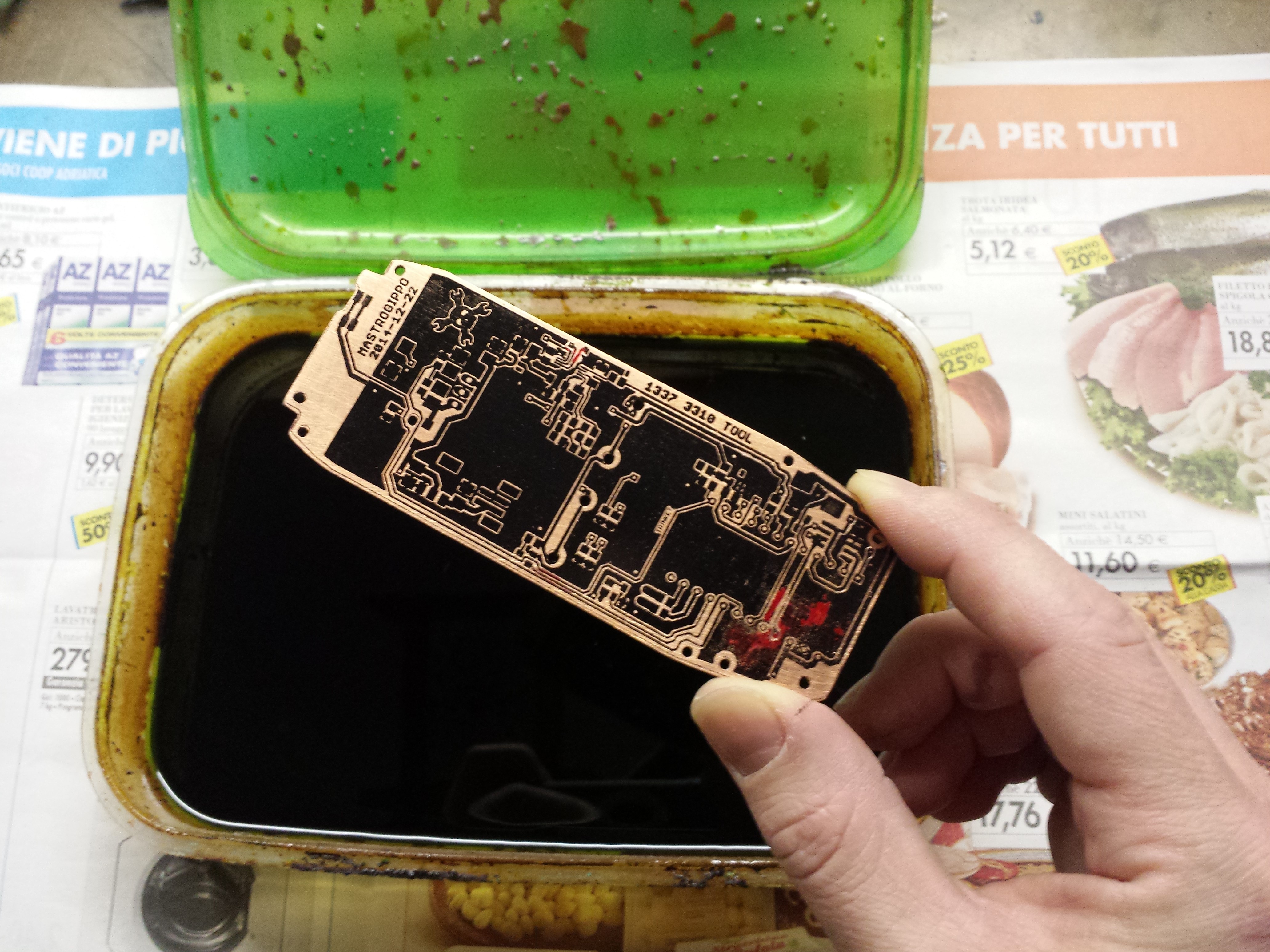
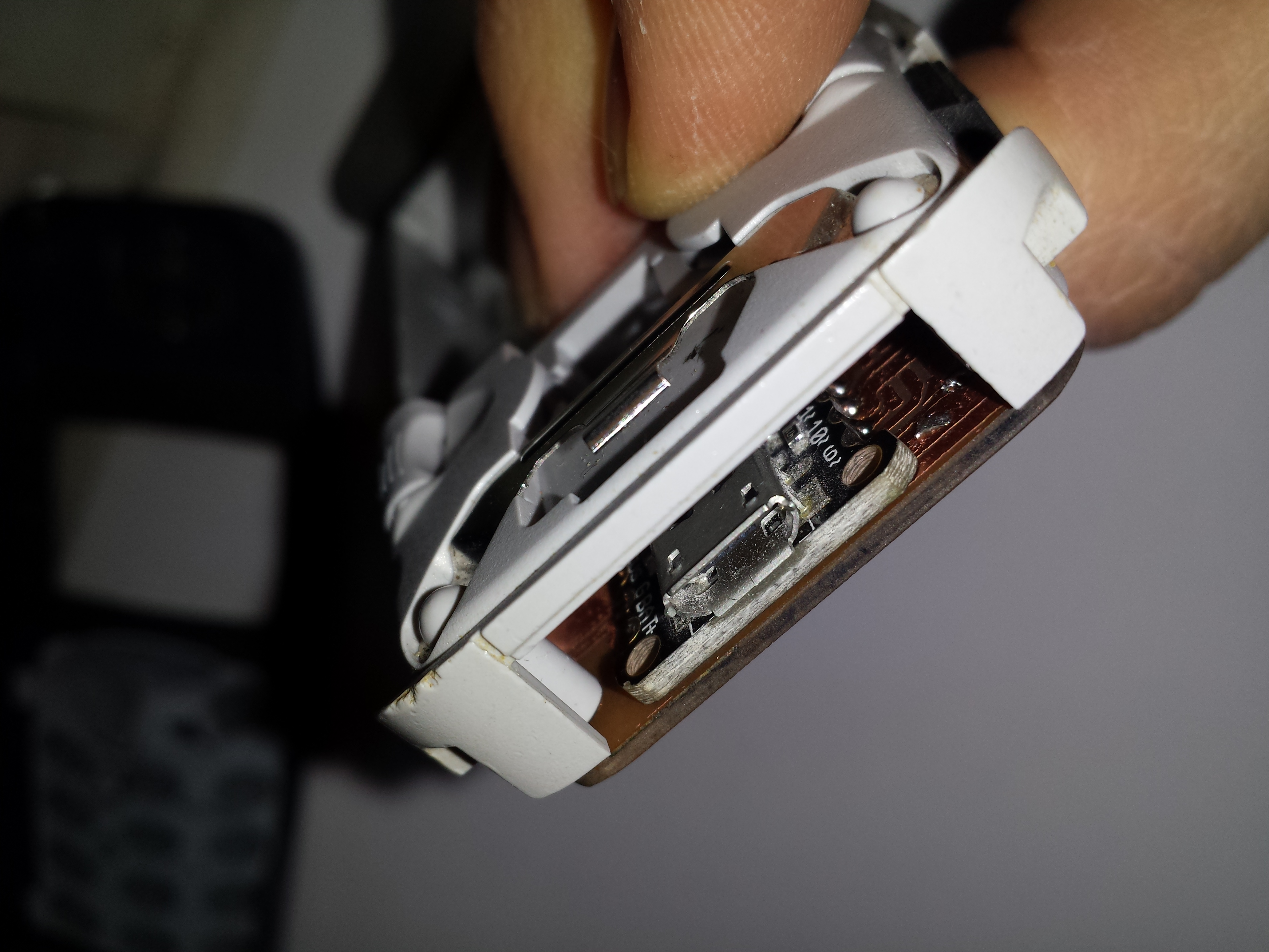
 it fit very well, despite the PCB being thicker than the original (1.4mm instead of 1mm).
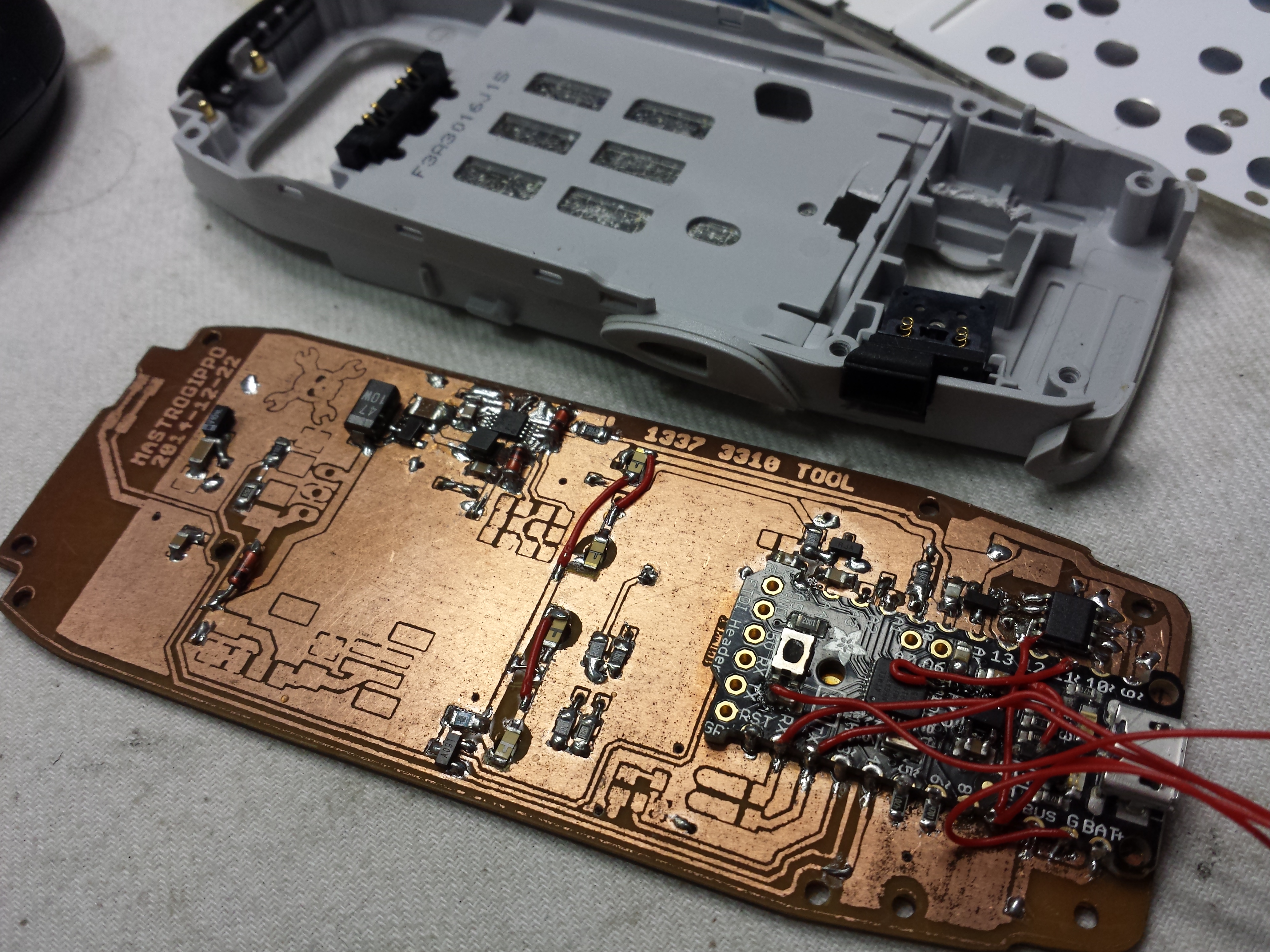
Time to fire up Eagle! I created a library for the phone footprint with the various pads for the LCD, buzzer, battery connector and buzzer and started laying out the board. I wanted to design a board that I could etch at home, so I had to stick with two layers, but I soon discovered that I had to give up the numeric pad to route all traces. I was still able to keep the function buttons, so I guess that I’ll live with that for now!
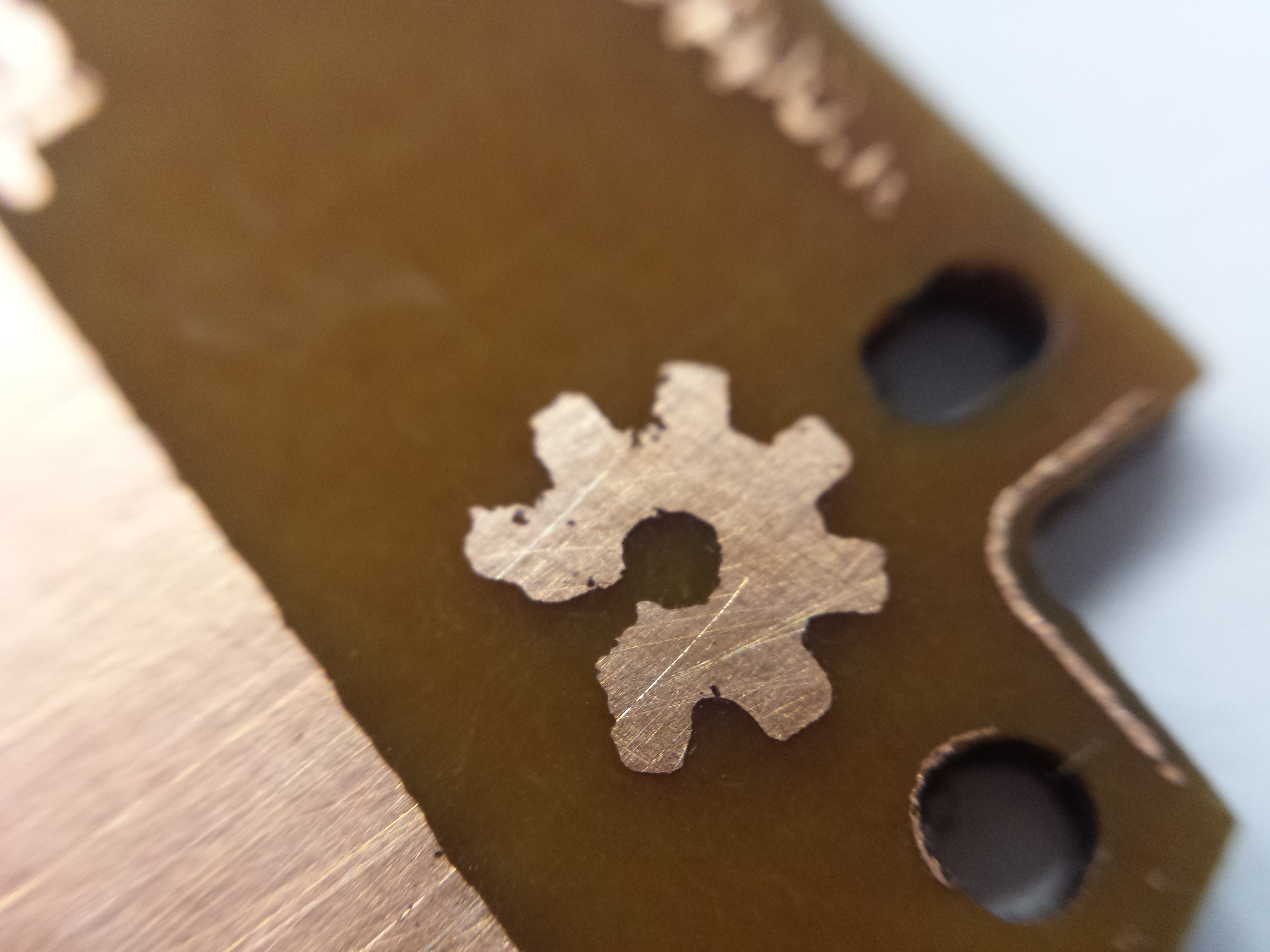
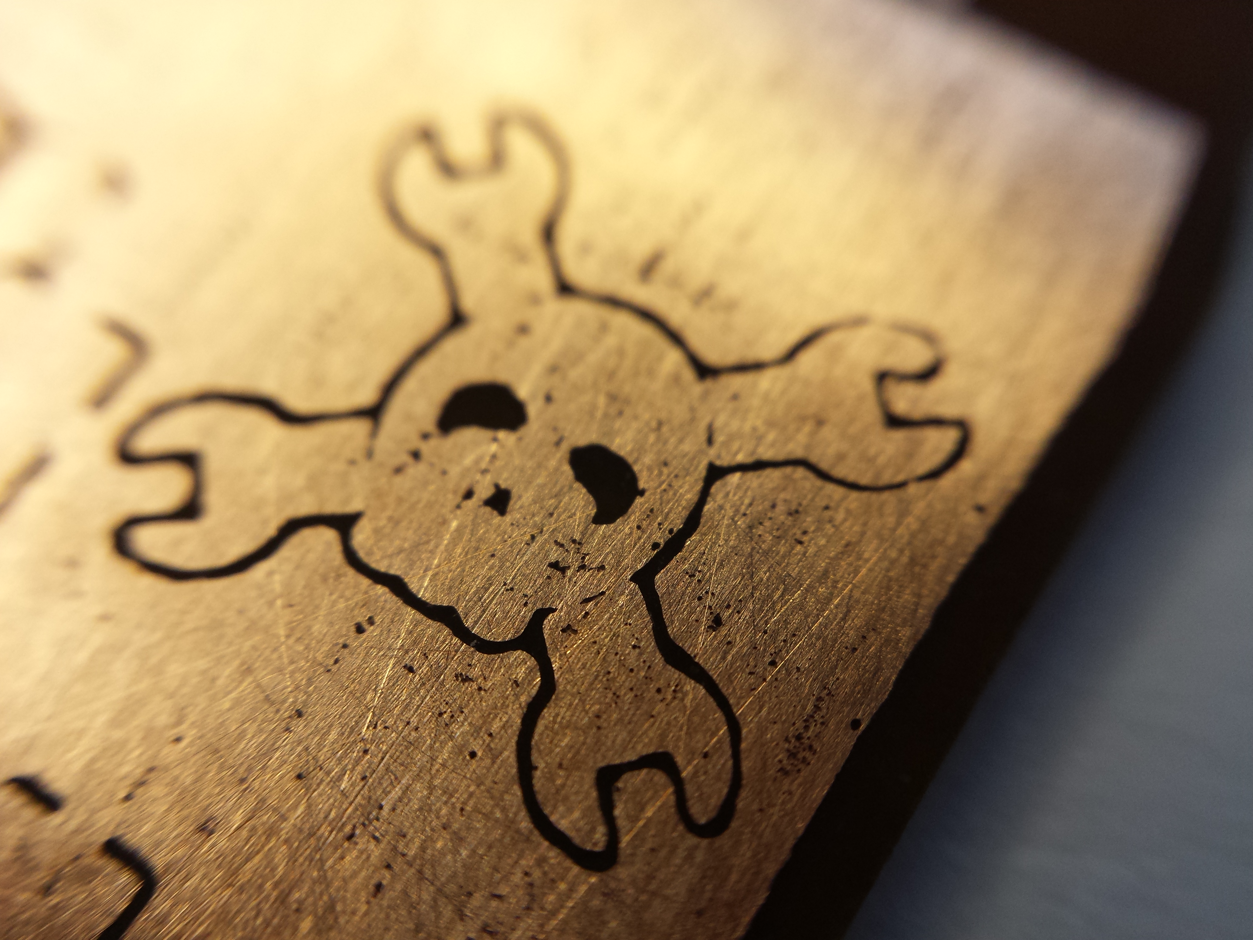
Etching the board was a nightmare by itself, as my printer couldn’t print a design this big on wax paper without scratching a lot of the toner away; Press’n’peel is not very good either for big boards with very thin traces. After dozens of failed tests, I was able to transfer the toner well enough with the good old photographic paper technique, being extra careful with every step of the process, even going as far as measuring the temperature of the iron before heating the board.

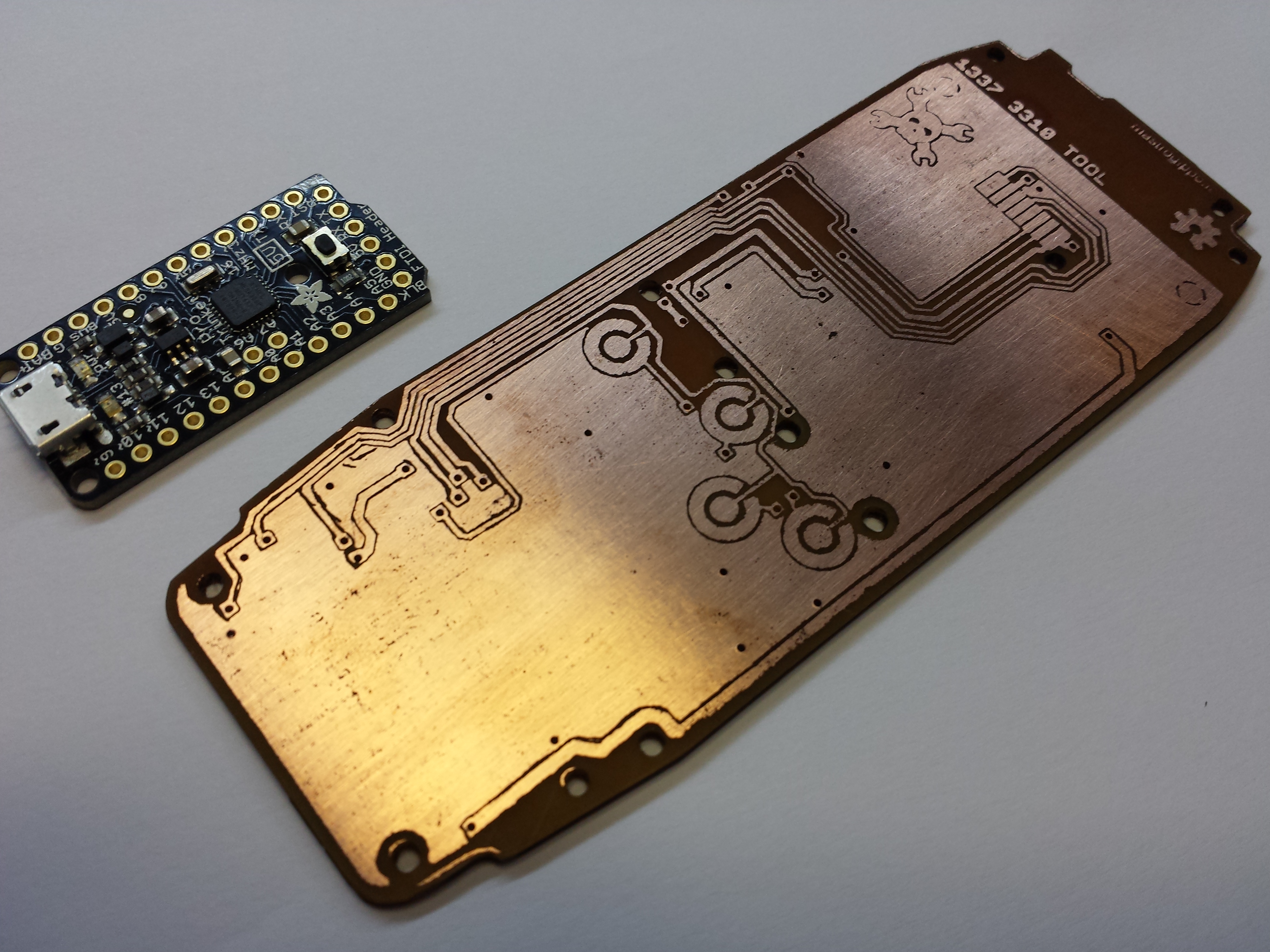
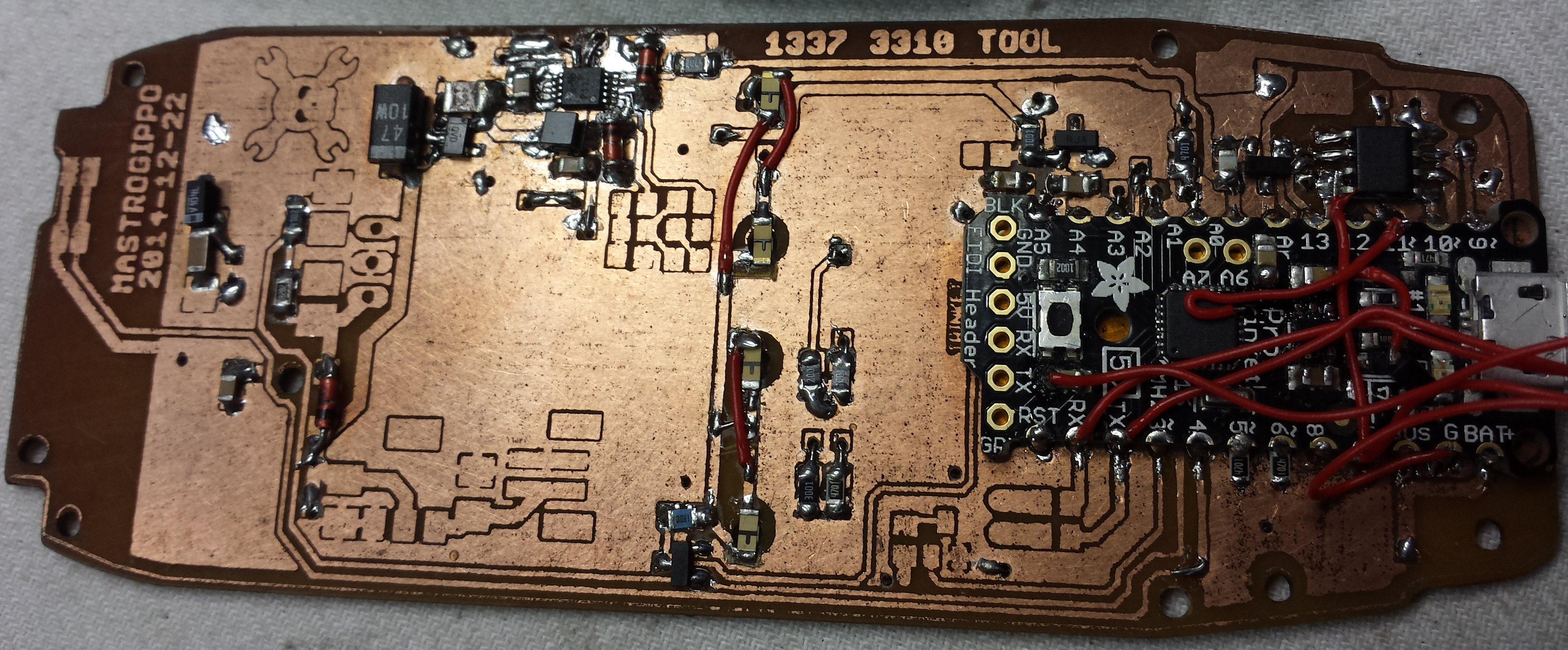
 TA-DAAAHHH!! Not perfect, but still very nice and usable. Since the board is sandwitched under the screen plastic frame, I couldn’t have anything protruding from the PCB, so I had to transform the Trinket to be surface solderable:
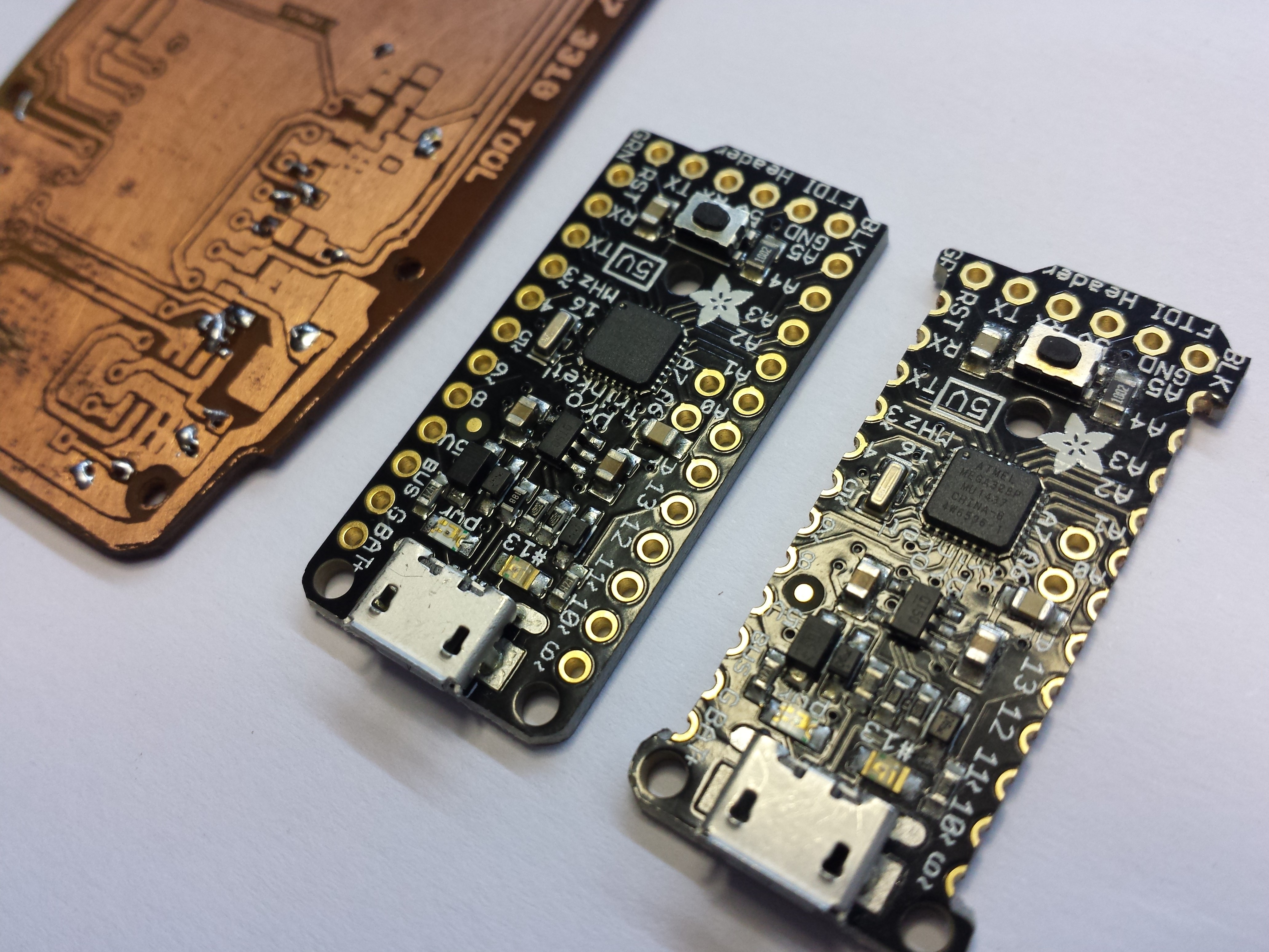
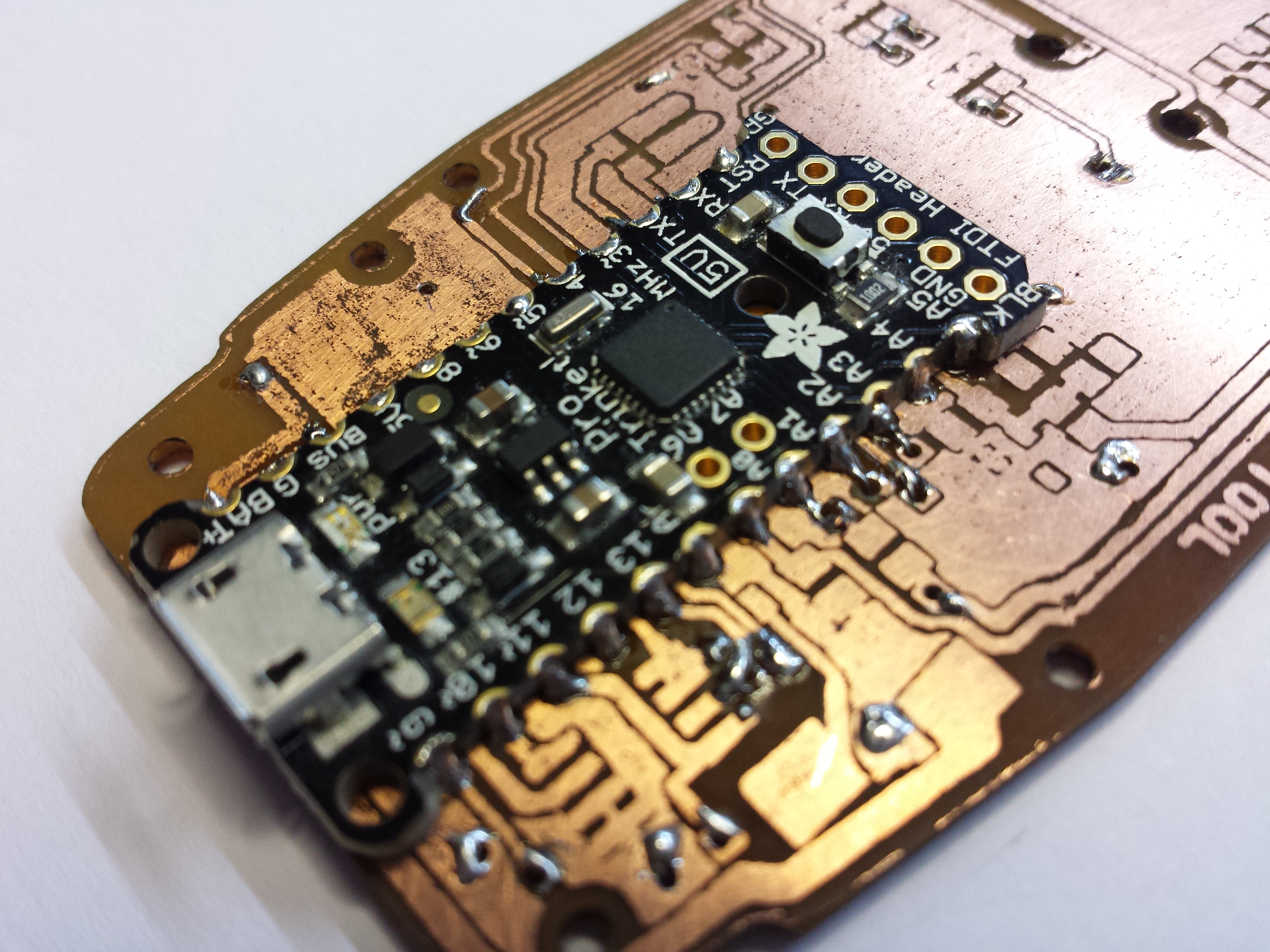
 Some filing and a bit of kapton to insulate the bottom pads, and I was good to go!
 Let’s write some software!