 This post is part of a series about this badge
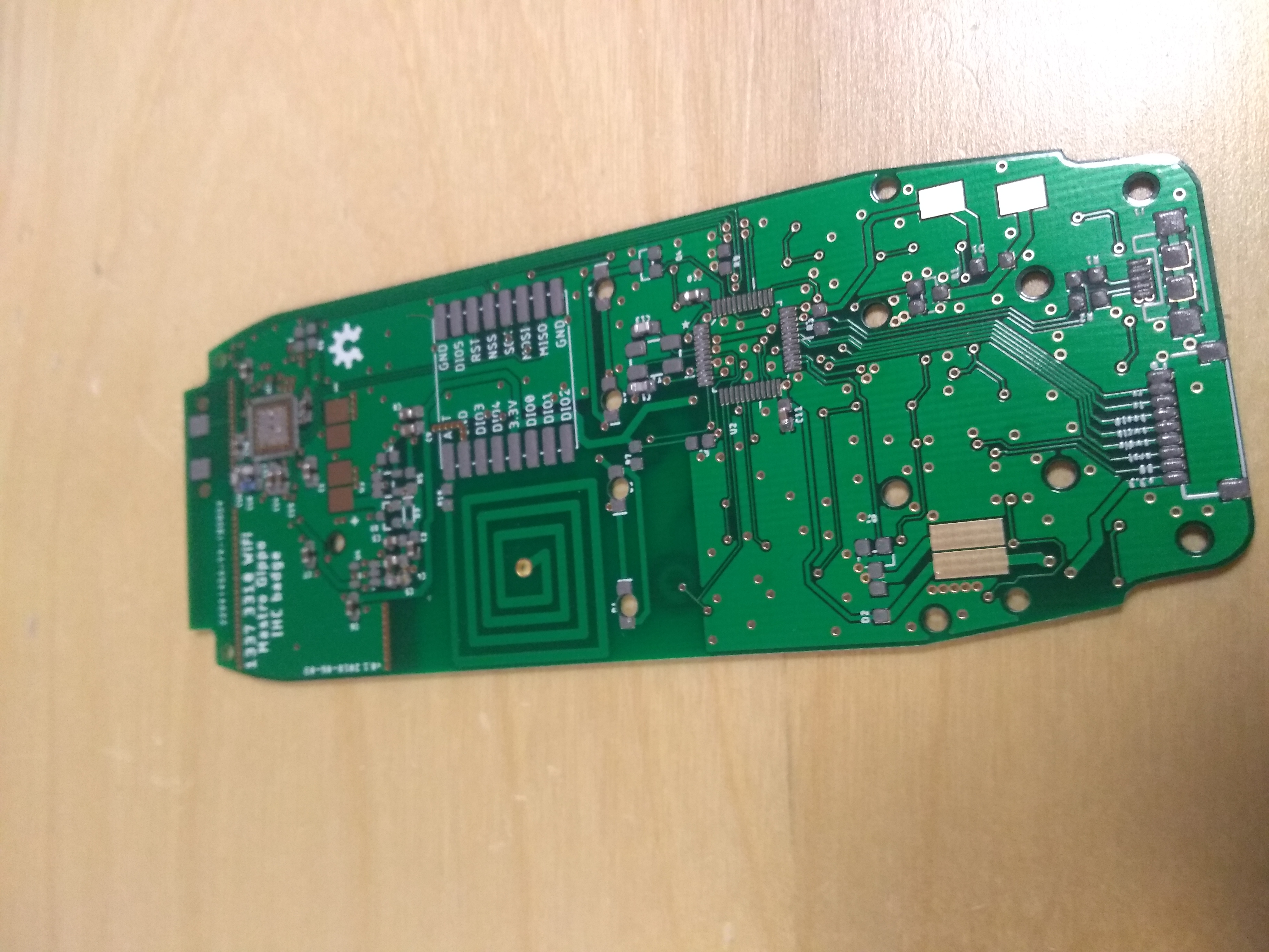
What goes into the design of a board like this? There’s a lot of choices to make when designing a circuit board, and I’ll try to tell you the story of how I went from the idea to the final design.
Design considerations

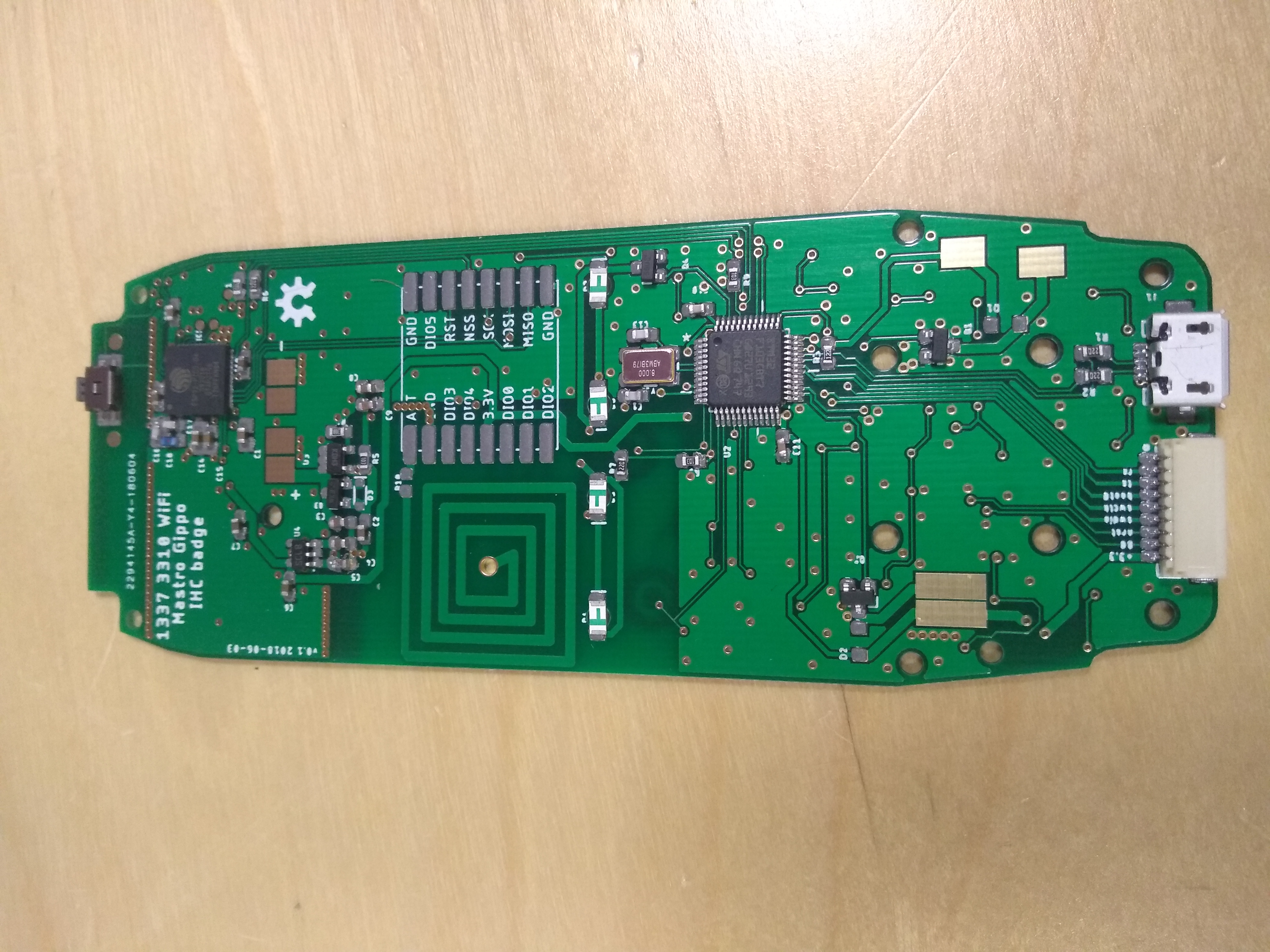
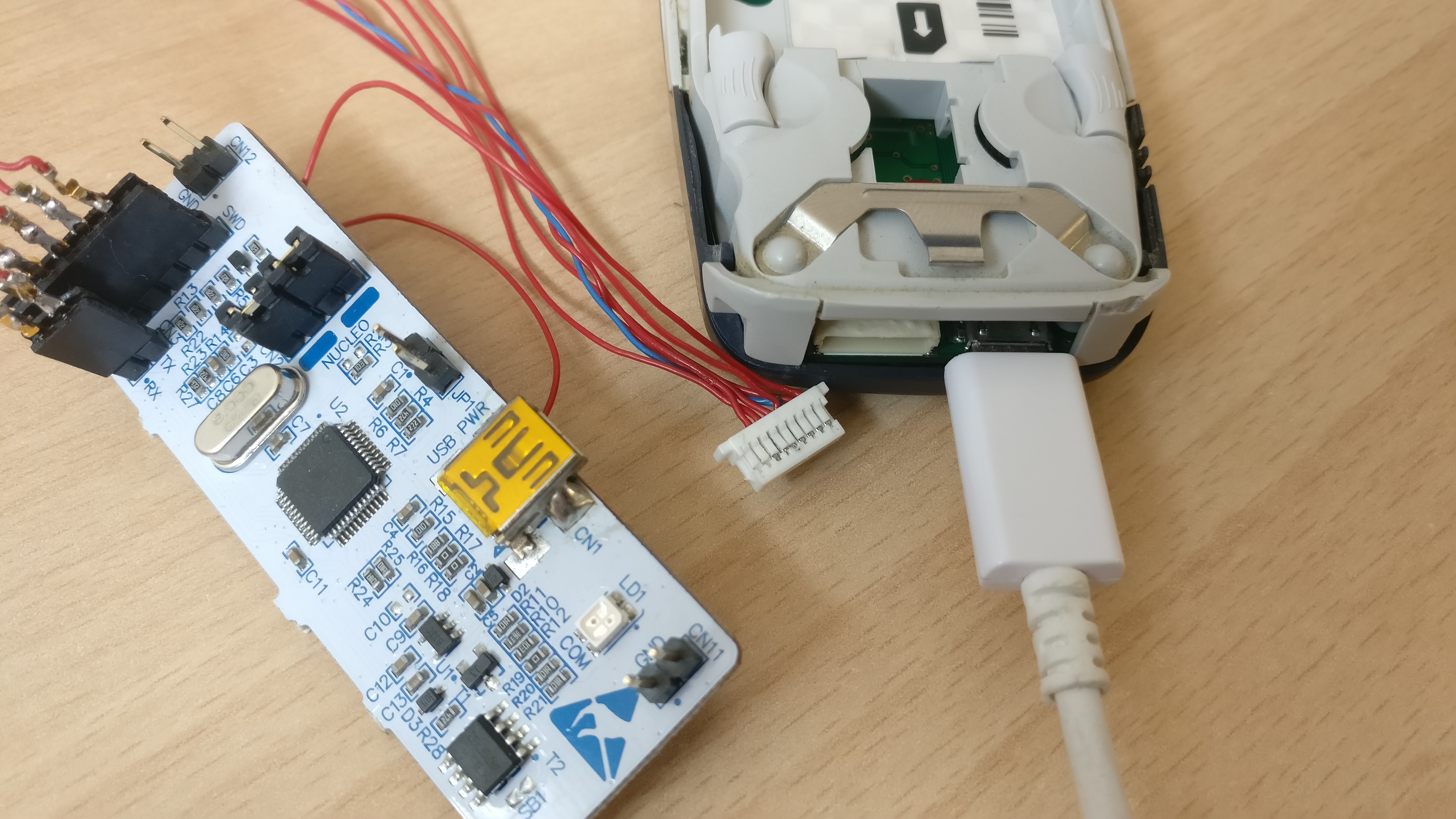
I thought a lot about how to interface the ESP32 to all the Nokia hardware. I2C IO expanders are a solution, but I would also have to add a USB-serial converter. Where’s the fun in that? An STM32 costs about the same and can do a lot more. So I went with it.
The programming serial port of the ESP32 is also sending and receiving peripheral data from the STM32. The STM32 holds the reset line to the ESP32 when it’s powered off. To boot the ESP32 in bootloader mode, you just have to power the phone on while pressing the “*” key. This solution is still not optimal, as I loaded the STM32duino bootloader on the STM32 so resetting via DTR-RTS only affects the STM32. This way you have to manually put the ESP32 in boot mode and remove the reset process from esp-load.py as that would reset the STM32 only. But at least it works! :)
Of course, after testing all the hardware, the first thing to implement was the RTTTL library to play the Nokia Grande Valse Ringtone!
I later added a cap and a resistor to filter the input to the mosfet driving the buzzer as the library leaves the pin high and this burns the buzzer.
The PCB form factor
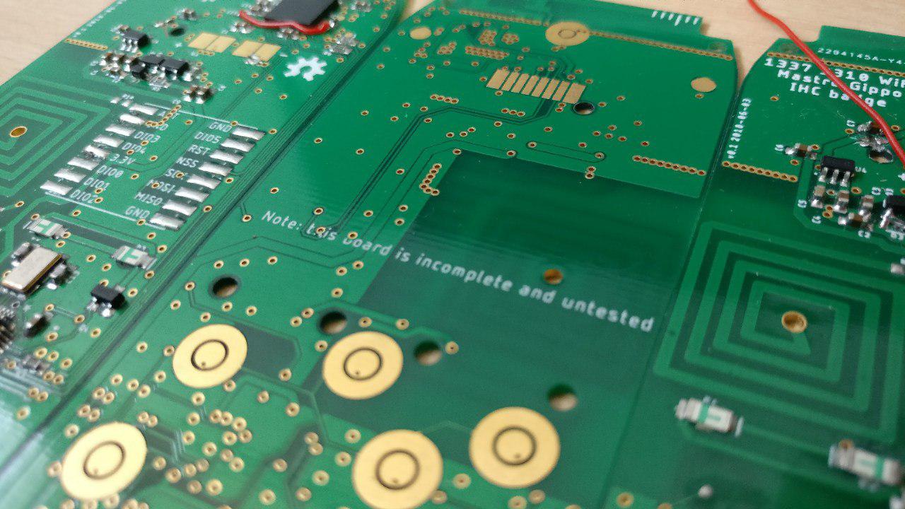
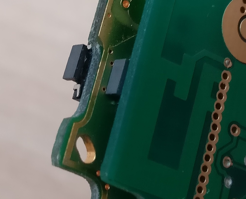
Since this board goes inside an existing enclosure (of which I didn’t have any specification or CAD drawing), the form factor is pretty constrained. Luckily, for this project, I stood on the shoulders of… well, me. The design still had to be completed and wasn’t tested with a factory-made PCB, so after a bunch of measurements and tests with printed paper I decided that it was time to bite the bullet and invest the ~100$ needed to manufacture the first batch of prototypes. JLCPCB proved reliable, fast and cheap as usual. Interestingly, they seem to post-process your designs: I used an ESP32-PICO footprint I found online and the solder paste mask was as big as the bottom pad of the chip. This would have been a problem as too much solder there would make the QFN “float” on the blob and the other pins wouldn’t reflow correctly; I didn’t notice this until the PCB assembly partner checked the design, but JLCPCB automatically corrected the problem for me (left chip):
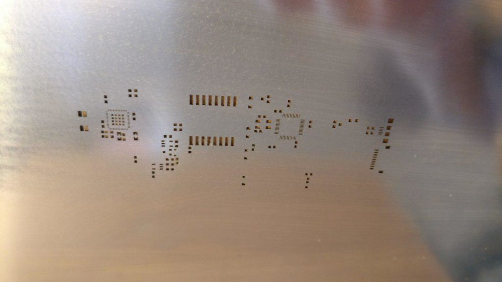
 Left: original footprint found online. Right: corrected one.
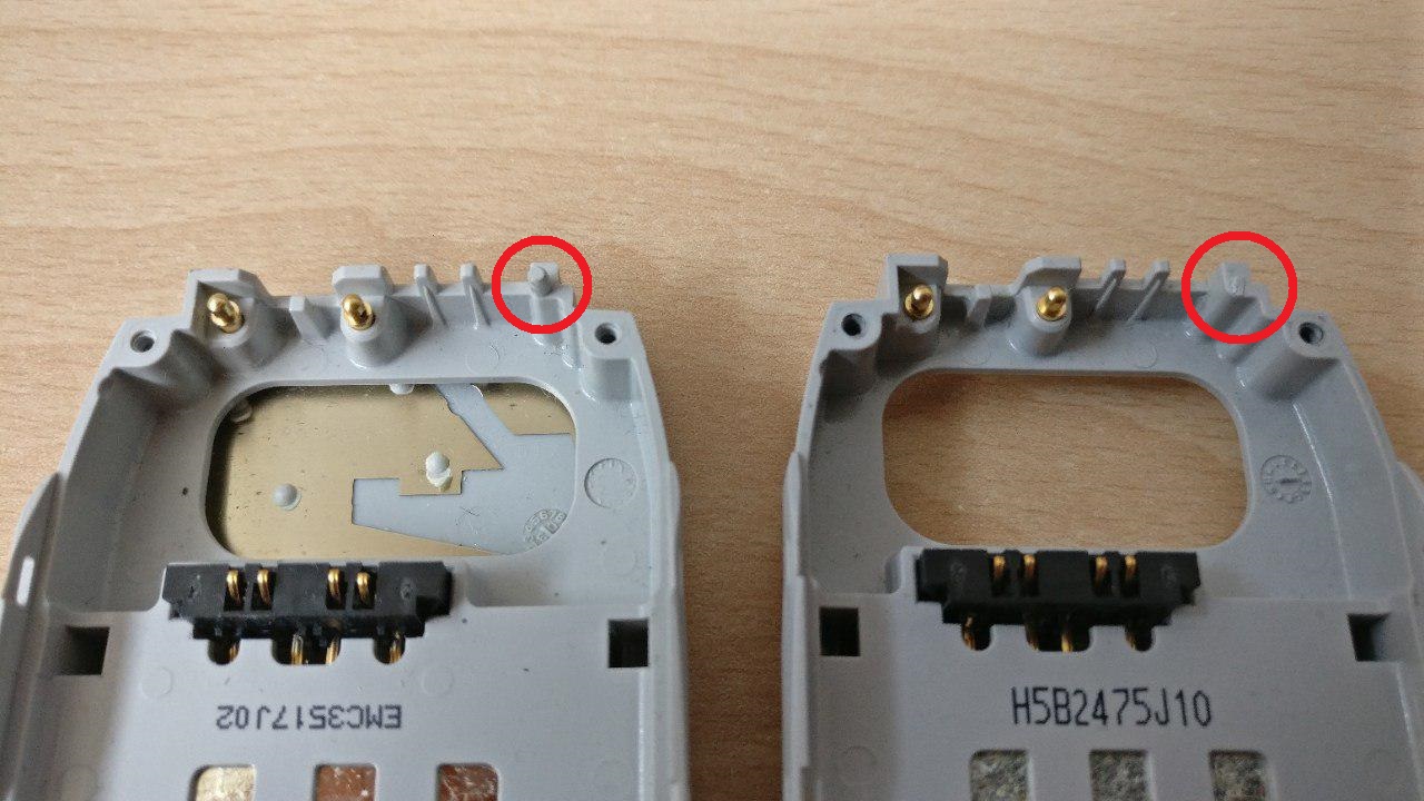
There is also a modification that I had to make to the case. I wanted to fit a big antenna on top of the phone, so I had to remove a plastic alignment pin because the hole to fit it would interfere with the antenna design. I’m really not proud of it, as I would have really preferred to keep it stock, but it’s a tiny modification that doesn’t interfere with the original board so I went with it.
Connectors
I was a bit worried that the PCB was too recessed into the plastic case to have a working USB connector, but luckily the micro USB connectors I’m using leave part of the plug exposed so a standard cable works well. There’s also a 9 pin JST connector for programming and expansion. Its pitch is very thin and almost impossible to crimp by hand though, and we couldn’t have cables made in time. Sorry – if you want to try to build your own cable, parts will be available at the camp.
Buttons
Gold plated buttons seem to work quite well, despite being super-bouncy. The great thing about a mass produced phone is that to save costs they “built” the buttons in the design, so I just had to design a few pads to make use of the 4×4 keypad.
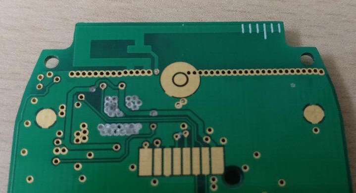
The power switch is a different, interesting story. I had to use the same exact switch to make sure that it worked well, so I started browsing Aliexpress to find a close match, looking for SMD edge buttons. Luckily enough it seems that these buttons are still in production, and they are made by Panasonic as EVQPUA02K. They’re available from Mouser too! Again due to antenna constraints, I flattened the original PCB inlet as it worked well even without it:
Antennas
The original idea was to copy the design of the ESP32-PICO-KITv4 with a Proant 440 metal antenna. This would have added cost so I started reading about PCB antennas, starting from the excellent Texas guide. I fell in love with the inverted F design and luckily found this great Eagle implementation by Fabio Altieri. It fitted exactly on the top of the PCB and is trimmable!
Here I must confess: I’m not an RF engineer. What I did was study a bit, google stuff, copy designs and guess component values. I guess I’m pretty lucky because it performed even better than the original design, finding 11 networks with good reception vs 8 with the ESP32-PICO-Kit.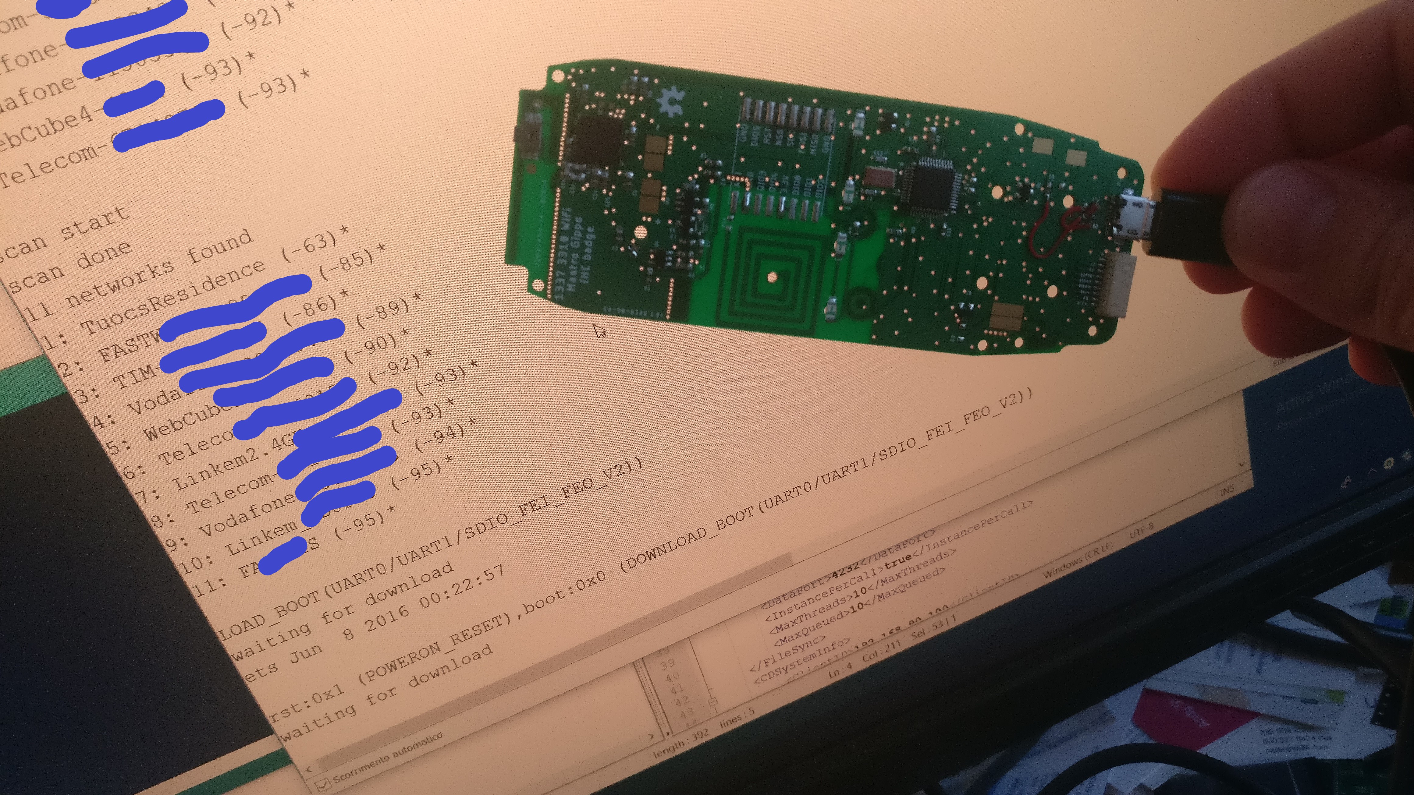
Another story is the LoRa Antenna. We decided to drop LoRa support but I already added the module to the design so I just left the footprint there and added a loop of wire of the approximate length as the 433MHz antenna. I didn’t test it, and I’m pretty sure it’s not going to work also because it’s pretty close to the metal battery, but on the new version there’s space for an U.FL connector if anyone wants to add its own RFM95W module and play with it.
An interesting idea would be to use the original Nokia antenna as 900MHz is quite close to LoRa’s 868MHz, but that’s left as an exercise for the reader.
Mistakes – 3 bodge wires
Despite carefully reading all the documentation I could find on the ESP32-PICO, I fell in the old trap of input-only pins. One pin of the ESP32 had to be rerouted for the display to work; I had enough experience that I could foresee this kind of problems so the design features a few spare pins broke out to pads that made the prototype modification pretty painless.
For the STM32 I was less worried, as I already designed a lot of PCBs with it, and of course I made the mistake of swapping D+ and D- for the USB connection because I copied it from a bad schematic found online. Damn.
Still, only 2 formal errors are not bad for this kind of board.
In the final version I also blindly swapped the LDO with an AMS1117, but as I went shopping for parts (after ordering 200PCBs of course) I found out that the AMS1117 has a high drop voltage, so it wouldn’t work when the battery was low on charge. Luckily I could find a device with a lower drop-out voltage that could fit in the same footprint.
Software
We’re working on it :)
Get it!
The badge will only be available to participants of IHC. I may run another batch and put it on Tindie or Crowdsupply; just send me an email to mastrogippo at mastrogippo.it if you want to be notified if/when I’ll put some on sale.
Hardware sources and schematics here
You can buy the assembled badge here, but I’d really prefer that you build it yourself from scratch and send me some pictures!! :)
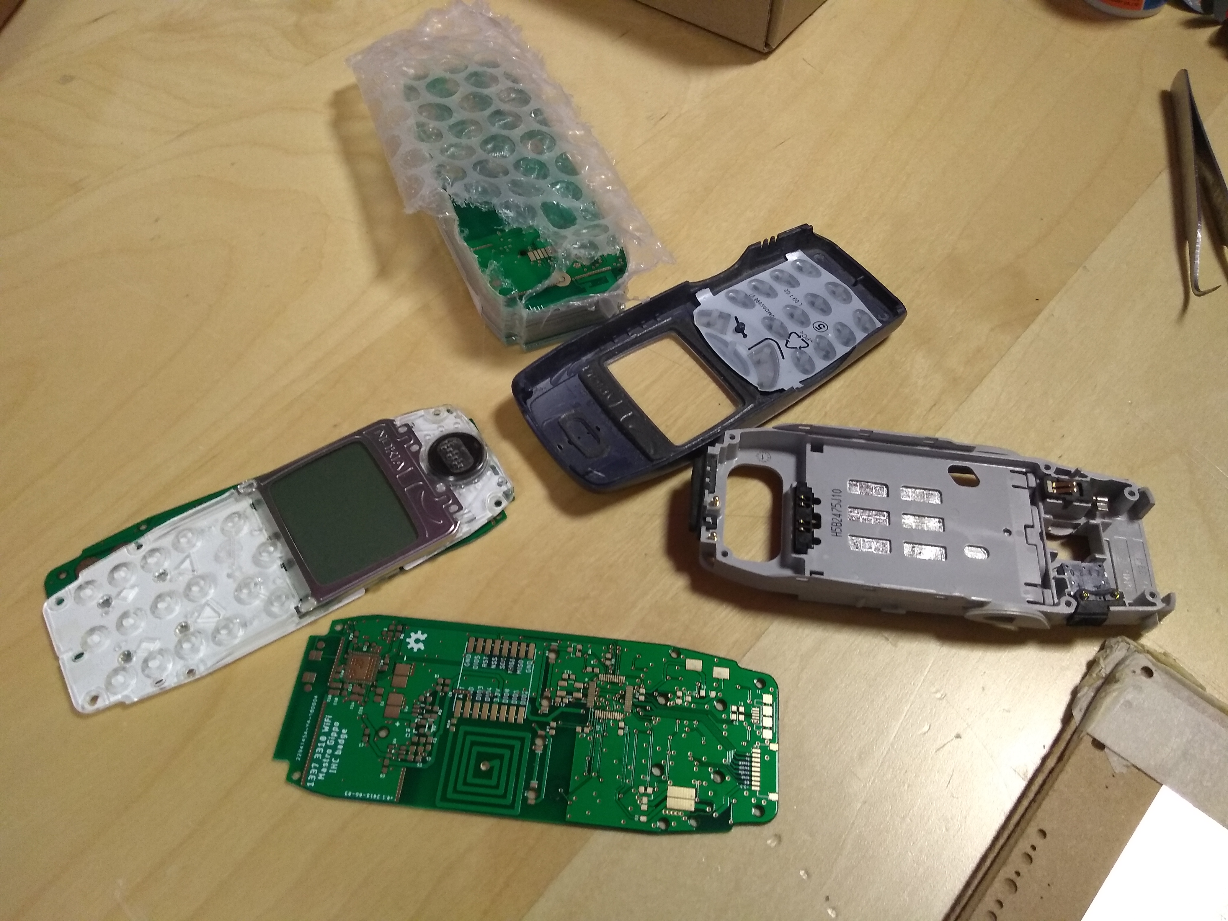
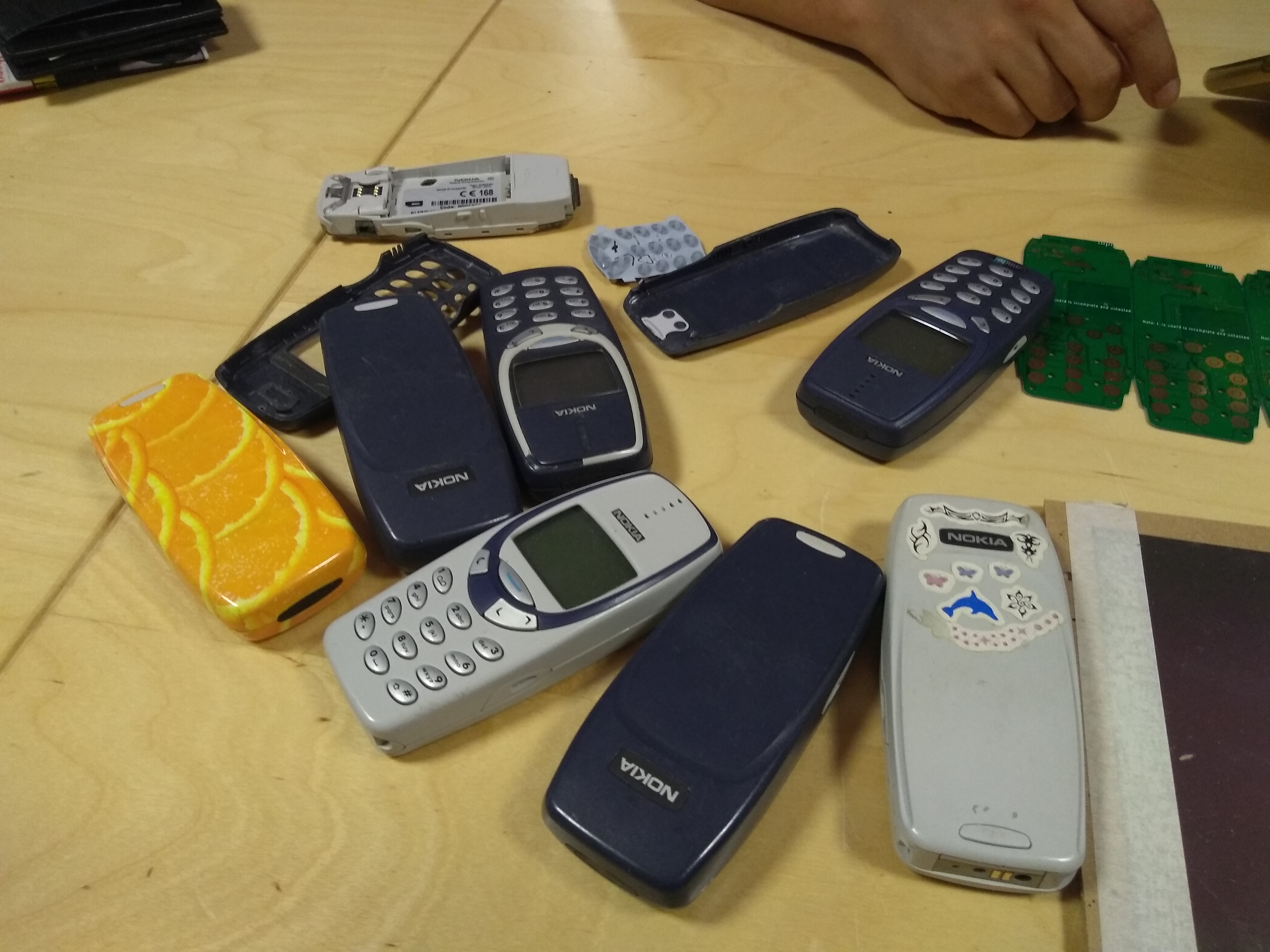
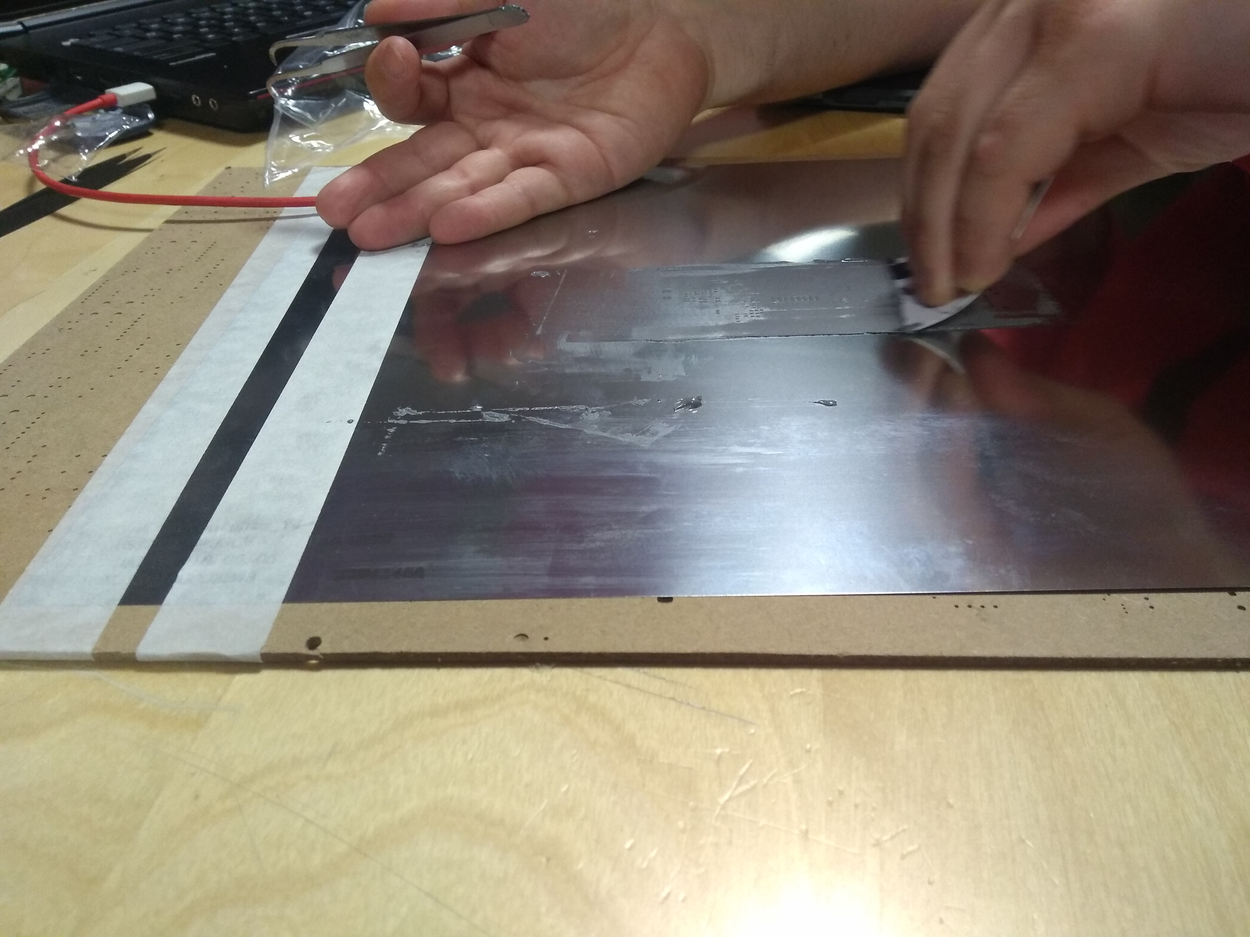
Random prototype assembly photos:
![]()